This thread has been locked.

If you have a related question, please click the "Ask a related question" button in the top right corner. The newly created question will be automatically linked to this question.

TAS5630BDKD dying unexpectedly

I am working with the TI TAS5630BDKD class D power amplifier on our own PCB layout. I have had to replace the IC twice due to it dying. The power supply current drops to zero and no audio out of the speaker output . This happens when trying to deliver full power into a 3 Ohm load at 1 kHz. The device does not go into shutdown it just dies. I am wondering if this could be due to inductors with high core loss or insufficient heat sinking. Although I would hope that the device shuts down instead of dying.

 I was wondering if anything come to mind. I can’t proceed with this design if this keeps happening as this may occur in products in the field. Any help would be appreciated.

Note that this problem does not occur on the TI eval board.

  • Hi John,

    Do you have the inductor spec? It is important to have at least 7uH of inductance under all operating conditions. Have you tried to use the EVM coil craft inductors and see if the IC still fails on your PCB?

    PCB layout is also critical for device reliability. DS page 25 PCB recommendation need to be followed. High freq decoupling caps, ground plane are important for reliability.

    Are you running BTL or SE? What is your supply voltage?


    reg,

    Paul.

    Applications Engineer


  • Hi Paul.

    John Wu at Arrow asked me to reply. The inductor is a custom made toroid made to the following specs: 7 uH nominal, 6 to 8 uH tolerance, Irms = 5A, 30 mOhm max DCR, core = micrometals T94-2. horizontally mounted on PCB.

    I have tried the EVM 7uh inductors at idel and draw 3x less supply current off 50 Vdc supply. I am in the process of trying them under the same 3 Ohm load.

    Will look again at layout, however, pretty sure we have followed the recommendations, lots of ground planes, 6 layer PCB.

    We are running in PBTL, same as was configured on EVM. Supply voltage is 49.9 Vdc form a TI 5122 master slave switching power supply.

    Could the device be heating up and dying without shutting down?

    I currently am trialing Coiltronics MA5173-AE inductors which were suggested by TI Application Engineer. They draw similar idle current as the 7 uH inductors from the EVM and will try them under load.

    Would a 10 uH value be a better fit to improve reliability?

    Best Regards,

    Steve Kempf

    steve.kempf@aem-corp.com

    1-250-763-1088 ext 347


  • An update:

    I tried using the inductors (7 uH) from the EVM and had the same failure in our PCB assembly. The device cuts out once. Then I lower the input level to correct the fault. When trying a second time to achieve full rated output into 3.5 Ohms, the device dies. After the failure: There is negligable current draw from the 50 Vdc supply. The SD pin is low, the OTW pin is high and the READY pin is low. An assertion of the reset pin does not affect the status of the error pins.

    I am using the same capacitors on the output that the EVM.

    Any suggestions as I am running out of options.

  •  

    Hi Steve,

    Does it get damaged when it is running at lower voltage? How close for the HF decoupling caps to the PVDD pins? Can you try moving the HF decoupling caps as close to the supply pins as possible? Maybe you can try measure the spike voltage at the output pins to see if there is excessive voltage spike due to layout.

    http://www.ti.com/lit/an/slea025a/slea025a.pdf

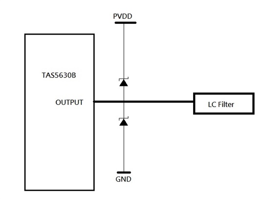
    Also you can try adding 30BQ060 surface-mount Schottky rectifier to the output pins (PVDD and GND). This is a 3A, 60V Schottky.  Here is the data sheet.  This diode or another with the same performance can be used.

    0003.6406.30BQ060-Schottky-60V-3A.pdf


    reg,

    Paul.


  • Thanks Paul,

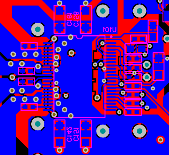
    The device only quits when the output is above 30 Vrms (1 kHz sine) into 3.5 Ohms. It is OK at lower rms levels. See attached image for HF coupling caps. They are at the top and bottom on the IC and are attached to a +50 Vdc power plane that runs under the IC (C142, C151, C158, C161) . I will measure the spike after I replace the device (again). Not sure if the layout for these caps is a problem?

    I am not clear where exactly the shottky should be connected. Could you please draw a napkin sketch or point me to a app note. Is it all four outputs (4 diodes)?

    Thanks for your help so far.

  • Hi Steve,

    Please see attached drawing for the diode placement. Put them on all 4 outputs. You may only need the GND diode. It really depends on the layout.  


    reg,

    Paul.


  • Hi Paul,

    Thanks for the schematic. Could I get away with a lower current handling device or is 3A continuous forward current rating required?

    Thanks,

    Steve Kempf

  • Hi Steve,

    You maybe able to get away with a lower current rating diode but it is really depends on your layout and how bad the spike voltage and ground bounce is.


    reg,

    Paul.