


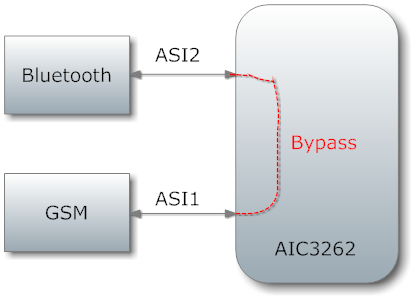
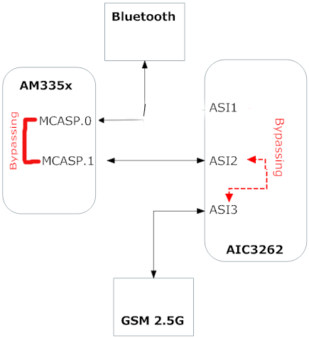
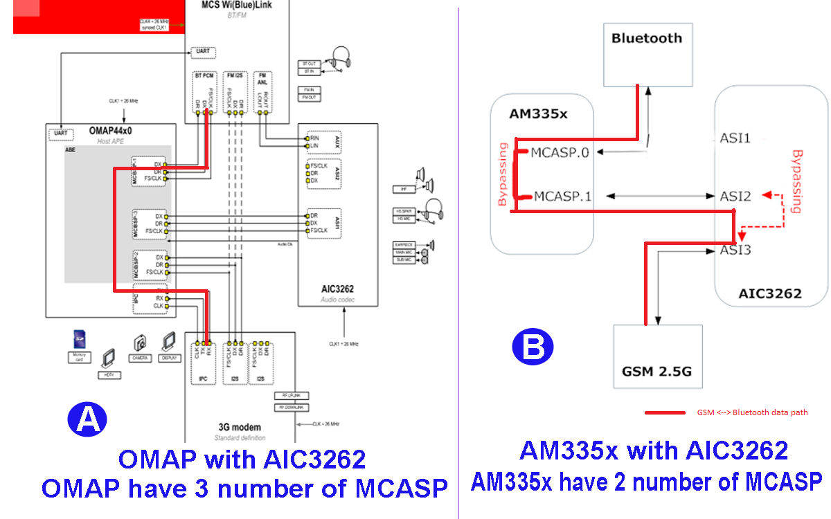
As we know AIC3262 have 3 number of independent audio serial interface.
I have the following question,
1. If i connect GSM audio in ASI1 and bluetooth on ASI2, if i get the call from GSM can i bypass the signal to bluetooth internally on AIC3262?
As we know AIC3262 have 3 number of independent audio serial interface.
I have the following question,
1. If i connect GSM audio in ASI1 and bluetooth on ASI2, if i get the call from GSM can i bypass the signal to bluetooth internally on AIC3262?


