This thread has been locked.

If you have a related question, please click the "Ask a related question" button in the top right corner. The newly created question will be automatically linked to this question.

TLV320AIC3262 ASI 4-channel using

Hello

Our customer wants to use two devices which have an audio serial I/O thru AIC3262.
Their signal flow is ASI2_in to ASI1_out mixing with ADC signal, ASI1_in to DAC and ASI2_out.
And they want to use AIC3262 as master device.

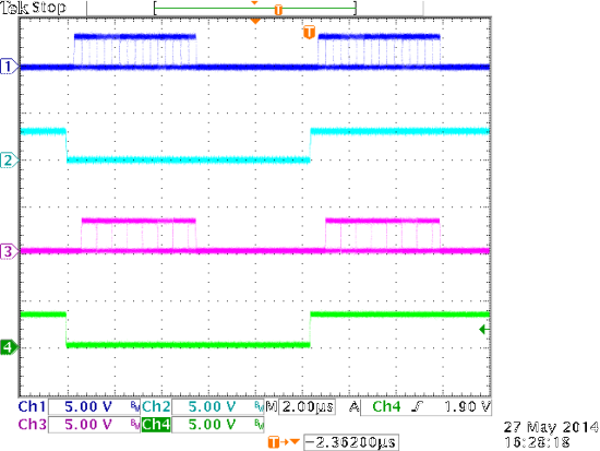
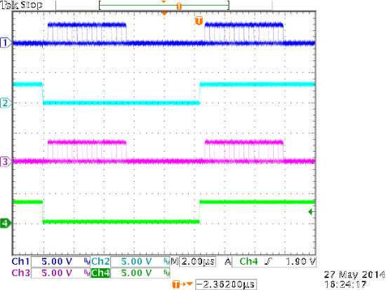
Now I'm trying it on PPS using two Serial Audio Interface #1 and Serial Audio Interface #2.
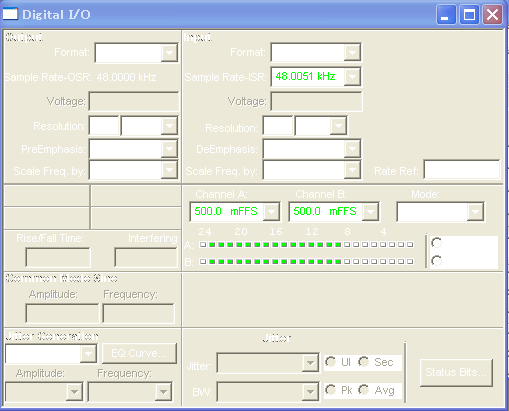
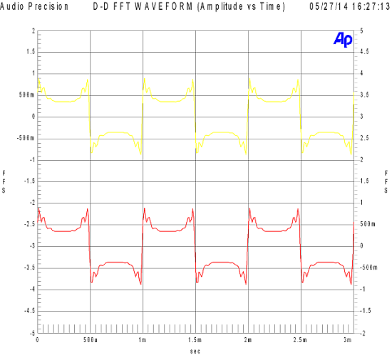
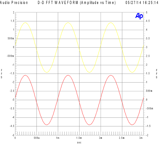
But I can't get clear output signal of SAI1_out and SAI2_out by AP with PSIA.

1st Question:
Is their signal flow possible, if AIC3262 is master and two audio signal interfaces are same sample rate?

2nd Question:
If the 1st Question is not possible, I want to propose that they use ASI1 as 4-channel interface.
But I2S_in and I2S_out component of PPS can be set as only 2-channel interface.
Please teach me the way to use ASI1 as 4-channel.

Best Regards,
Ito

  • Hi, Ito-san,

    I've asked my colleague to work with you on this issue. But, he is out of the office today. I expect him back tomorrow.

    -d2

  • Hi Ito,

    Yes, it is possible to use the configuration you proposed in the signal flow.

    You would need to configure the ASI settings in the SystemSettingsCode property of the framework. The ASI1 and ASI2 must then need to be set as I2S master. Refer to the Applications Reference Guide for details on how to configure the ASI busses.

    Thanks,

    J-

  • J Arbona-san,

    Thanks you for variable suggestion.

    But I already confirmed that AS1 and AS2 can be set the clock master by execution of a cfg as shown below,
    instead of SystemSettingsCode property of the framework.

    # select page 0
    w 30 00 00
    # Select Page 4
    w 30 00 04
    # ASI1_BDIV_CLKIN = DAC_MOD_CLK
    w 30 0B 01
    # BCLK N divider powered up
    # BCLK divider N = 2
    w 30 0C 82
    # ASI2_BDIV_CLKIN = DAC_MOD_CLK (Generated On-Chip)
    w 30 1B 01
    # Secondary BCLK N divider is powered up
    # Secondary BCLK divider N = 2
    # B0_P4_R28 =0x82
    w 30 1C 82
    # Bit Clock Output = ASI1 Bit Clock Divider Output
    # Word Clock Output = Generated DAC_FS
    w 30 0E 00
    # Bit Clock Output = ASI2 Bit Clock Divider Output
    # Word Clock Output = Generated DAC_FS
    w 30 1E 20
    # WCLK1 pin is output from Audio Serial Interface 1
    # BCLK1 pin is output from Audio Serial Interface 1
    w 30 0A 24
    # WCLK1 is ASI1 Word Clock Input/Output
    w 30 41 04
    # DOUT1 is ASI1 Data Output
    w 30 43 22
    # DIN1 is enabled for Primary Data Input
    w 30 44 20
    # WCLK2 pin is output from Audio Serial Interface 2
    # BCLK2 pin is output from Audio Serial Interface 2 Bit Clock
    w 30 1A 24
    # WCLK2 pin acts as ASI Secondary WCLK as defined in B0_P4_R26_D5
    w 30 45 04
    # BCLK2 pin acts as ASI Secondary BCLK as defined in B0_P4_R26_D2
    w 30 46 04
    # DOUT2 pin Output = ASI2 Data Output
    w 30 47 22
    # DIN2 Enabled
    w 30 48 20
    # All Channels of Data Input on DIN1 pin
    w 30 05 00
    # All Channels of Data Output on DOUT1 pin
    w 30 06 00
    # ASI2 digital audio output data is sourced from ADC miniDSP Data Output 2
    w 30 17 05
    # ASI2 Left DAC Datapath = Left Data
    # ASI2 Right DAC Datapath = Right Data
    w 30 18 50
    # Independent Left and Right Channels for ADC miniDSP output
    # DAC miniDSP Data Input 1 receives data from ASI1 output
    # DAC miniDSP Data Input 2 receives data from ASI2 output
    w 30 76 06


    The BCLK and WCLK when AS1 and AS2 are set the clock master is below.

    Is the SystemSettingsCode property setting of the framework necessary
    even if executing the cfg file at the reset?

  • J Arbona-san,

    I took the data more in EVM.
    Are the following the result of not to set the SystemSettingsCode property of the framework?
    The data are not transferred from AS1 to AS2 definitely. A sign bit of MSB seems to be missing.

    The Digital I/O window of Audio Precision.


    AS1 and AS2 wave form.
    blue : AS1 Data Output
    cyan : AS1 WCLK (master)
    magenta : AS2 Data Output
    green : AS2 WCLK (master)


    AudioPrecision FFT Waveform of the AS2 input data

    The signals when PSIA output to input loop-back are shown below as reference.

  • J Arbona-san,

    The AS2 Data Output must be the same as AS1 Data Input signal.
    Why do the data not accord?
    Will the registers setting be wrong?

    best regards,
    Ito

  • Hi Ito-san,

    Please refer to the SystemSettingsCode snippet below as a reference. It configures ASI1, ASI2 and ASI3 as I2S master. Note that the BCLK N divider value may be different depending on your clock tree setup.


    ;--------------------------------------------------------------------------------------------
    ; ASI1 Configuration
    ;--------------------------------------------------------------------------------------------
    ; Format: I2S
    ; Data Width: 32-bit
    ; BCLK: 3.072 MHz
    ; WCLK: 48 kHz
    ;--------------------------------------------------------------------------------------------
     reg[  0][  4][0x01] = 0x18 ; I2S Format, 32-bit, DOUT1 3-state off               
     reg[  0][  4][0x02] = 0x00 ; Offset = 0                                         
     reg[  0][  4][0x07] = 0x01 ; ASI1_in = miniDSP_A(L1,R1)                       
     reg[  0][  4][0x08] = 0x50 ; miniDSP_D L1 = left, miniDSP_D R1 = right     
     reg[  0][  4][0x0a] = 0x25      ; WCLK1/BCLK1 are ASI1 outputs, always powered
     reg[  0][  4][0x0b] = 0x01      ; ASI1_BDIV_CLKIN = DAC_MOD_CLK
     reg[  0][  4][0x0c] = 0x82      ; ASI1 BCLK N = 2, powered on
     reg[  0][  4][0x0d] = 0x20      ; ASI1 WCLK N = 32, powered off
     reg[  0][  4][0x0e] = 0x00      ; ASI1_BCLK_OUT = ASI1_BDIV_OUT, ASI1_WCLK_OUT = DAC_FS
     reg[  0][  4][0x0f] = 0x00 ; DOUT1 = ASI1_DOUT                                
     reg[  0][  4][0x43] = 0x22 ; DOUT1 pin enabled, used for ASI1_DOUT              
     reg[  0][  4][0x44] = 0x20 ; DIN1 pin enabled, used for ASI1_DIN

    ;--------------------------------------------------------------------------------------------
    ; ASI2 Configuration
    ;--------------------------------------------------------------------------------------------
    ; Format: I2S
    ; Data Width: 32-bit
    ; BCLK: 3.072 MHz
    ; WCLK: 48 kHz
    ;--------------------------------------------------------------------------------------------
     reg[  0][  4][0x11] = 0x18 ; I2S Format, 32-bit, DOUT2 3-state off               
     reg[  0][  4][0x12] = 0x00 ; Offset = 0                                          
     reg[  0][  4][0x17] = 0x05 ; ASI2_in = miniDSP_A(L2,R2)                          
     reg[  0][  4][0x18] = 0x50 ; miniDSP_D L2 = left, miniDSP_D R2 = right           
     reg[  0][  4][0x1a] = 0x25 ; WCLK2/BCLK2 are ASI2 outputs, always powered        
     reg[  0][  4][0x1b] = 0x01 ; ASI2_BDIV_CLKIN = DAC_MOD_CLK                       
     reg[  0][  4][0x1c] = 0x82 ; ASI2 BCLK N = 2, powered on                         
     reg[  0][  4][0x1d] = 0x20 ; ASI2 WCLK N = 32, powered off                       
     reg[  0][  4][0x1e] = 0x20 ; ASI2_BCLK_OUT = ASI2_BDIV_OUT, ASI2_WCLK_OUT = DAC_FS
     reg[  0][  4][0x1f] = 0x00 ; DOUT2 = ASI2_DOUT                                   
     reg[  0][  4][0x20] = 0x00 ; ASI2_ADC_WCLK = ASI2_WCLK, ASI2_ADC_BCLK = ASI2_BCLK
     reg[  0][  4][0x47] = 0x22 ; DOUT2 pin enabled, used for ASI2_DOUT               
     reg[  0][  4][0x48] = 0x20 ; DIN2 pin enabled, used for ASI2_DIN    

    ;--------------------------------------------------------------------------------------------
    ; ASI3 Configuration
    ;--------------------------------------------------------------------------------------------
    ; Format: I2S
    ; Data Width: 32-bit
    ; BCLK: 3.072 MHz
    ; WCLK: 48 kHz
    ;--------------------------------------------------------------------------------------------
     reg[  0][  4][0x21] = 0x18 ; I2S Format, 32-bit, DOUT3 3-state off               
     reg[  0][  4][0x22] = 0x00 ; Offset = 0                                          
     reg[  0][  4][0x27] = 0x06 ; ASI3_in = miniDSP_A(L3,R3)                          
     reg[  0][  4][0x28] = 0x50 ; miniDSP_D L3 = left, miniDSP_D R3 = right           
     reg[  0][  4][0x2a] = 0x25 ; WCLK3/BCLK3 are ASI3 outputs, always powered        
     reg[  0][  4][0x2b] = 0x01 ; ASI3_BDIV_CLKIN = DAC_MOD_CLK                       
     reg[  0][  4][0x2c] = 0x82 ; ASI3 BCLK N = 2, powered on                         
     reg[  0][  4][0x2d] = 0x20 ; ASI3 WCLK N = 32, powered off                       
     reg[  0][  4][0x2e] = 0x40 ; ASI3_BCLK_OUT = ASI3_BDIV_OUT, ASI3_WCLK_OUT = DAC_FS
     reg[  0][  4][0x2f] = 0x00 ; DOUT3 = ASI3_DOUT                                   
     reg[  0][  4][0x30] = 0x00 ; ASI3_ADC_WCLK = ASI3_WCLK, ASI3_ADC_BCLK = ASI3_BCLK
     reg[  0][  4][0x4b] = 0x22 ; DOUT3 pin enabled, used for ASI3_DOUT               
     reg[  0][  4][0x4c] = 0x20 ; DIN3 pin enabled, used for ASI3_DIN  


     Regards,

    Jorge

  • J Arbona-san,

    Thank you for a reply.

    I appended to SystemSettingsCord your script.

    Now I am testing it.

    The signal pass of AS1 to AS2 is good, but a signal conflict occurred on DOUT1 pin.

    It may be a problem only for my EVM, because my EVM cannot play the music of PC via USB now.

    However, the DAC of my EVM outputs the signal when I input I2S signal into headers of AS1 directly.

    regards,

    Ito