


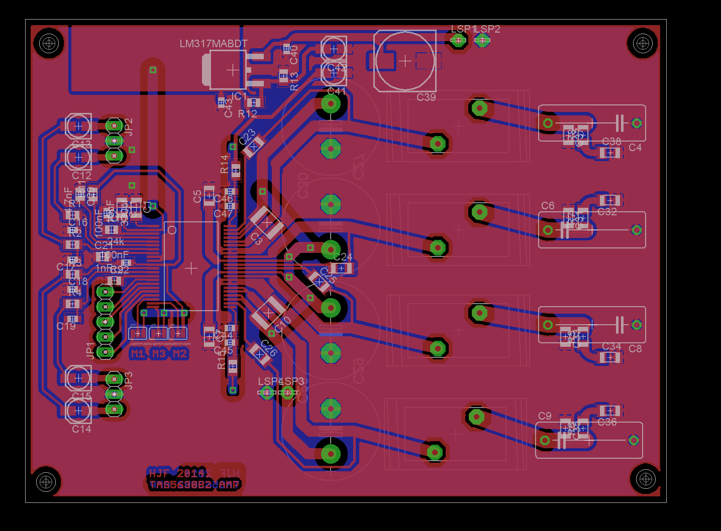
I'm working on a layout for TAS5630B. For reasons outside my control (taxes, import restrictions, exchange rate and time), right now I can't afford to have boards made at a factory. So I'm forced to make my own PCBs at home. I can only make single-sided, or single sided + a very simple design on the bottom with no metalized holes.
So, the reference design is out of the question since it uses thin traces, tight spacing, and very small alignment tolerances.
This is the best I came up with, for a double-sided design with only a few traces in the bottom side, the rest being GND:
(larger here: http://i.imgur.com/sttiJCA.png)
I tried to get the decoupling capacitors (C3, C5, C7, C10 2.2uF 100V) as close as I could to the power pins. I read it also needs to have 10nF and 100nF capacitors in parallel to these. So I thought of just mounting these on top of the SMDs. I don't mind the extra work as this board is not intended for production.
With this board I aim to get at least 100W on a 4 ohm load (mono). I don't plan on running it near the chip's limits (400W!), so I estimate the supply voltage needed will be about 30-35 volts.
Extra question: is the ouptut RC network strictly required or is it for EMI reduction purposes only?
