This thread has been locked.

If you have a related question, please click the "Ask a related question" button in the top right corner. The newly created question will be automatically linked to this question.

Problems of TAS5421

Other Parts Discussed in Thread: TAS5421-Q1

Hello,

I have some problems to the reference schematic of TAS5421 as belows:

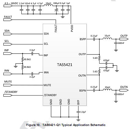
1.If we want to replace the LC filter with ferrete bead in BD mode(our application is 4W).How can we choose this ferrete bead?

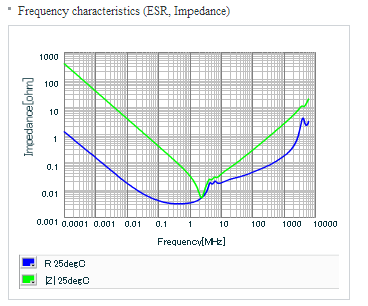
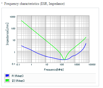
2.For the input pi filter, why so strange combination(2.2nF,82nF,4.7uF*2,10uH,0.1uF,1uF) are used?How can we choose according to our application?(with GSM/GPS module, SMPS around 1MHz)

Please help solve my confusion about this, thanks!

Best Regards,

Junwen Yuan

  • Hi Junwen:

    Thank you for your interest in TAS5421-Q1.

    It seems that you got the application schematic from an older data sheet version (preliminary).  Can you please tell me where you get this version?  TAS5421-Q1 has been released for production and the application schematic has been updated.  It is available on TI web site.

    What is your end product for using TAS5421-Q1?  Do you have to meet certain EMC requirements?

    We test EMC at 1W for CISPR 25 Class 5 and the LC filter is needed.

    For the PVDD input, it is recommended that .1uF close to the PVDD pin for high frequency filter for the device, 10uF and 330uF next to 0.1uF by PVDD pin is for bulk capacitance.

    The 10uH along with 2x 4.7uF, 82nF and 2.2nF are for EMC filtering both radiated and conducted.  We put these on the EVM close to the input connector for CISPR 25 class 5 requirement.  If your system power supply already has EMC filter suppression that meets your system requirement then they are not needed.

    Please see the documents on the web page here:

    http://www.ti.com/lit/ug/slou365/slou365.pdf

    http://www.ti.com/product/TAS5421-Q1/technicaldocuments

    Best regards,

    Tuan

  • Hello Tuan,

    Thanks for your reply!

    We are now working on telematics. The preliminary datasheet was provided by some FAE in Ti.

    I'm always feeling puzzled about the problem I posted before.Actually, from my understanding, 4.7uF suppress noise from 1MHz~10MHz, 82nF suppress noise from 10MHz~100MHz, and 2.2nF more than 100MHz. I don't know if I'm right or not? Why don't you put all these capacitors after the inductor?(Cause there's always reverse battery protection diode in front)

    For 4.7uF:

    For 2.2nF:

    Have you consider the TDD noise(around 217Hz)?

    Also,why you said this filter will also be good to radiated disturbance? In my limited understanding, it has only work conducted noise.

  • Hello Yuan:

    The reason for the PVDD LC filter setup on the EVM is to stop the PWM switching going back out to the power line.  If you have a method that works for you, do keep it.  The device switches at 400kHz and 500kHz so make change to the filter for appropriate switching frequency and its associated harmonics.

    For automotive requirement, we test for CISPR 25 Class 5 which starts at 150kHz mono pole.  The filter for PWM output and PVDD input are selected such that they pass both RE and CE.

    Best regards,

    Tuan