This thread has been locked.
If you have a related question, please click the "Ask a related question" button in the top right corner. The newly created question will be automatically linked to this question.
Hello,
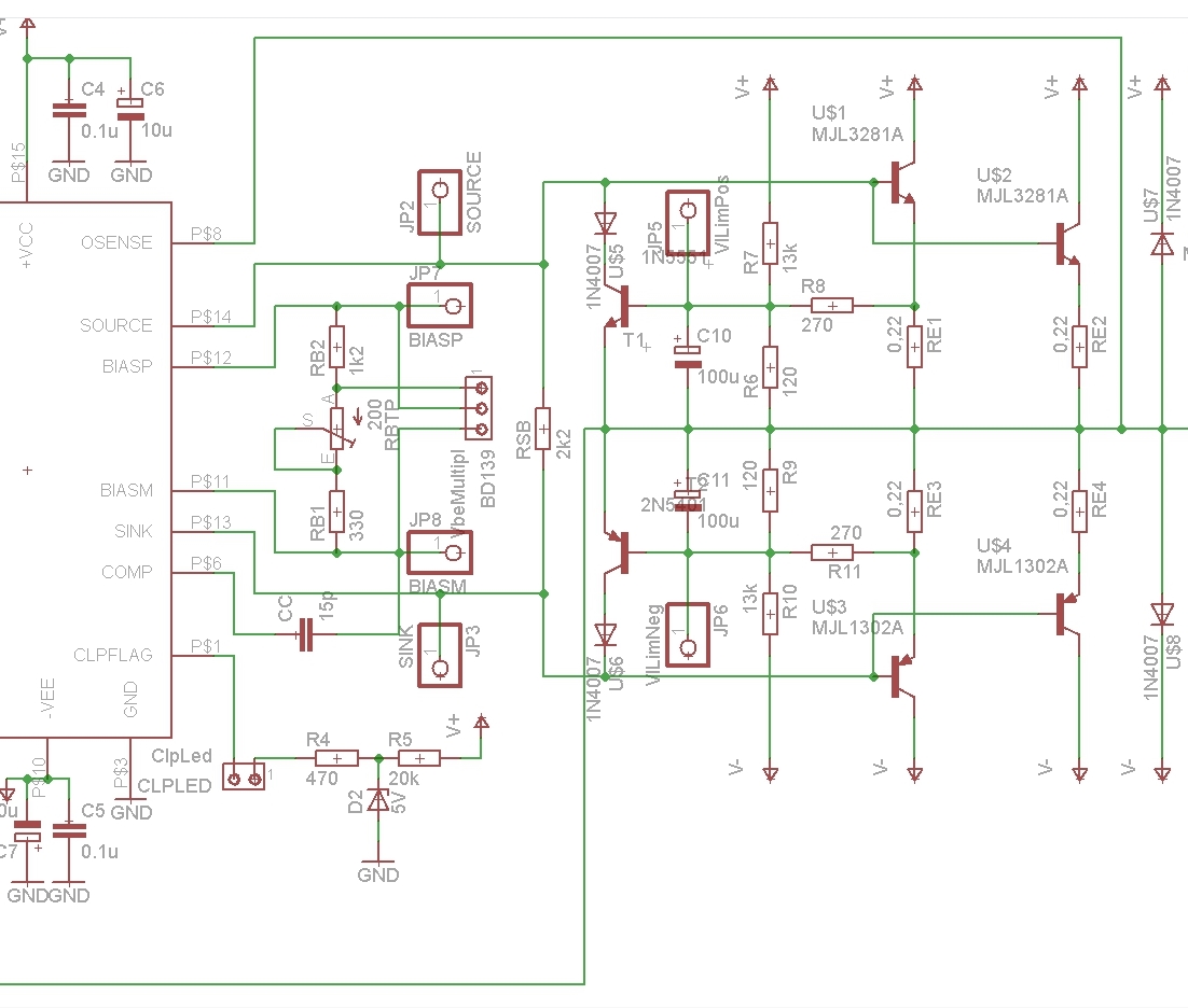
I am trying to use single slope VI limiting on a BJT Output stage driven by the LME49180.
The last time I turned it on I ruined the OPS Transistors and also the LME49810 started smoking. I checked my wiring over and over but could not find an error. Has anyone had this problem or was it really an erroneous connection on my breadboard?
Without the single slope VI limiting circuit the amplifier runs perfectly well.
Thanks for your answers!
Hello Michele-san,
Can you show your single slope VI limiting circuit? Then I can make proper advise for you.
Best regards
T NAOKAWA
Hello Michele-san,
Thank you for providing your schematic. I'll make some comment on your connection as below.
The output current on "Source" and "Sink" pins are 60mA typ and hs no upper limit. If your current sense transistor sensed output current and try to reduce base current of output power transistor, the current sense transistor has to handle close to 60mA or more. In this case, LME49810 Source or Sink output transistor consume high power consumption and with out heat sink, the die temp of LME49810 may exceed 150 degC or higher and as the result, Source or Sink output Tr may have damage and then sensing transistor may have damage. To avoide this kind of operation, I'll suggest that the collector of current sensing transistor connect to Biasp and BiasM via diode. Then the current limit will work as you expected.
Please try that way.
Best regards
T NAOKAWA
Hello Naokawa-san,
I have tried your suggestion and it works so far.
I just want to make shure if I understood your advice correctly.
When too much current or voltage ist detected, for example the current limiting transistor T1 in the schematic below will become conductive, which in turn withdraws current from the biasp pin. Since the biasp pin is internally connected to the base of the driver transistor of source it will withdraw that current. This way the Base current to the OPS Transistor is limited.
Well I thank you very much for your advice, it has really helped me!
Sincere Regards
Michele Lucchi
Hello Michele-san,
It is good to hear from you that it worked.
Yes, your understanding is correct. When T1 detected current flowing on RE3, T1 start conductive and then the collector pull BiasP current which is about 2.8mA. As the result internal base current of emitter follower for Source will be reduced and then output cirrent of source is limitted and then external power Tr's drivability will be limitted. It is same manar for Sink side.
Best regards
T NAOKAWA