Hello
I had checked DRV612 EVM to compare the ' Fail ' sample ' (Gain= 16dB from customer's board )
and 'Good 'one (Gain=3.5dB) when Rgain=51Kohm.
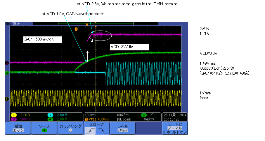
Attached is the 'Good' sapmle (EVM) wave form.
We see some glitch ( internal circuit start up and seems proper operation for internal charge pump something )
when Vdd is over 2.8V at ''Good' sample.
Also, when Vdd is over the 1.9V , GAIN voltage goes up.
Here is the question.
Q1 Is these waveform proper operation? ( Would you please check in TI USA?)
Customer had found there are no glitch on GAIN terminal on ' Fail' sample on customer's board, but
found glitch on 'Good' sample.
Q2 Would you please describe how DRV612 internal circuit works at the Power up for Gain-setting?
I need more detail internal block diagram for DRV612 also.
Customer is using DRV612 for their STB from a few years ago, but they found 3pcs/1500pcs were illegal gain (16dB, all of 3pcs)
even Rgain=51Kohm.
I have doubt for customer's board( noise of Vdd line)
Best Regards