This thread has been locked.

If you have a related question, please click the "Ask a related question" button in the top right corner. The newly created question will be automatically linked to this question.

TPA2013D1 drawing too much current

Other Parts Discussed in Thread: TPA2013D1EVM, TPA2013D1, ALLIGATOR

I received a TPA2013D1EVM today (my 2nd one in a month).  The first one worked well for awhile, but then suddenly the 8-ohm speaker I had connected to it melted.  I tried another speaker ... same thing.  Since I had used these speakers before, I assumed something was wrong with the EVM.

With the replacement EVM today, I connected it to a known good 8-ohm speaker.  Powered the EVM with a 3.8V supply.  And connected it to a 1kHz sine wave (measured the sine-wave to be 400mVp-p into a high impedance load).  Gain is set to 6V/V, which is the default.

Turned on the power, and measured 0.7A average current.  That's WAY too much current.  Turned it off quickly, don't want to destroy any more speakers because I know what will be coming if I continue to test.

Given that this is the 2nd EVM that has failed (and although on the first one I didn't at the time that it failed measure current, the symptoms of melting speakers would be consistent with too much current going into the speaker), I'm trying to figure out what the issue could be. 

This EVM was right out of the box and into the lab, and behaved this way from the moment that it was first powered. 

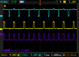
Without a speaker connected, I've measured again the voltages and everything looks fine. 

Has anyone else seen TPA2013D1 fail in a way that causes them to draw excessive current? 

Any ideas what the problem could be and why I seem to be so unlucky as to have had a poor evaluation experience with both amplifiers that I tried.

  • Hi, Richard,

    Welcome to e2e, and thanks for your interest in our products. You don't mention the power rating of your speaker, is it greater than the 2.7W rating of the TPA2013D1?

    Can you try using a resistive load, and measuring the waveforms to see if they correspond to the ones published in the data sheet?

    -d2
  • My speaker is a 1W speaker, which I realize is quite small for what the TPA2013D1 can do. I had hoped to use the TPA2013D1 because it is able to boost 1.8V (when my battery ... 2-cell alkaline ... is near terminal voltage) up to something that is still able to deliver 1W to my speaker without clipping and distortion.  Can't afford the space I would need for a 3W speaker.

    But it shouldn't matter, with a 400mVp-p and 6 V/V gain, the rms power on paper should be around 0.09W, right?  Long way from the limit of the speaker. 

    I will measure with an 8-ohm resistor tomorrow, but I have observed that no load, the current isn't excessive.

  • This is what a snapshot of the waveform looks like with a 4-ohm load (I couldn't find a large enough 8-ohm resistor).  Current is 1.5A average (and seems to be that no matter what my input is (same current if I'm playing the 1kHz sine wave versus if I don't have any input applied at all).

    And here it is with no-load.

    Channel 1 is OUT- and Channel 2 is OUT+ (both measured with respect to ground).  Seems a bit odd to me that when I do the math (CH1-CH2 ... I know, technically it should be the other way around), that there is a dc-offset.  Not sure what it is supposed to look, but I would have expected a dc-offset of 0V.  CH2 looks suspicious.

  • Should also add that with no input at all, Channel 2 is at ~5V. Neither it nor Channel 1 toggle at all, with no input (and the current is constant, around 1.5A). Seems to me the one FET is stuck high.

    Both this EVM, and the previous one that this one was to replace, behave exactly the same. This one has been that way from the get-go (the other one at least used to work just fine for quite some time).

    Probing at IN+ and IN- on the chip, with no input connected, I see that IN+ is at a dc-offset (presumably an internal bias) but IN- is stuck low. Shouldn't IN-, with no input, be biased to the same dc offset as IN+?
  • Hi, Richard,

    Sorry for the delay. Please confirm that you have the speaker connected between VOUT+ and VOUT-? There should be no connection to ground.

    -d2
  • Hi, Richard,

    If you have the speaker connected between VOUT+ and VOUT-, can you make plots of the outputs with zero input signal, and then with a full-scale 1 kHz sine wave? I'd like to see if the PWM output is changing.

    -d2
  • I most certainly do (and did) have the speaker connected between VOUT+ and VOUT-. GND was never involved (other than the alligator clip on my oscilloscope which was connected to J1 as a common reference).

    It really isn't worth me attaching a plot, I can describe it pretty well. With zero input signal, I see no transitions at all. VOUT+ is stuck at 5V, VIN- is stuck at 0V.

    With an input sine-wave (1kHz, 1Vp-p ... though this detail doesn't matter because I can't really capture enough data with my oscilloscope to filter out the high-frequency switching components from the output to see a sine-wave, even if the amplifier was working), I see bursts of activity that are the same as the "zero-input state" I describe above, and bursts of activity that appear like the screenshots I've already attached (VOUT+ and VOUT- toggling between 5V and 0V according to some sort of varying pattern).

    The RCA input to the EVM is connected to a XLR output from a StellarLabs speaker tester (through an XLR to RCA adapter). I don't have any other non-default jumpers installed on the EVM (in particular nothing on J8 ... worth noting that I think).

    I only recently acquired this Stellar Labs speaker tester.

    Before that I was using an iPod. Again, I was simply connecting the headphone output from the iPod through a passive adapter cable into the RCA input of the EVM. Couldn't as easily modify the voltage as I can with this new speaker tester I'm using, but I had measured with an oscillscope and the peak-to-peak signal I could get on the RCA cable (not connected to the EVM) was about 2.5V. On the EVM, there was no jumper on J8 at all ... even though the audio input was technically "single-ended" and not "differential" ... I reasoned to myself that the iPod audio output referenced to its "GND" ... then ac-coupled to the amplifier ... could float relative to the EVM board's "GND" and that was all still ok (and I still would believe that to be the case, unless you can explain to me otherwise ... why the EVM would need a common ground with the audio source).

    I think the evidence that I've seen indicates this EVM (and the other one before it) have something gone strange with the amplifier. I have measured the IN- input (relative to GND on J1) between C9 and U1, and it is low ... I would have expected it to have the same dc-bias as IN+ measured between C10 and U1 (which appears, at least now, to be around 800mV with zero input). Because IN- appears to be "stuck low" rather than dc-biased to be equal to IN+ ... that creates a differential voltage at the input to the amplifier, and that dc-voltage then appears at the output of the amplifier ... hence the reason that VOUT+ minus VOUT-, even with zero input, is not a zero output.

    So at this point, I need to figure out why, when I've tested two different EVMs, both ended up with this same failure mode (one right away, one after a couple days of normal use), and how it is that the high-impedance IN- input of the amplifier can be stuck low. I know the EVM (both of them) must be fried. I can't move forward and select this part knowing that this failure mode exists, without understanding what I've done (assuming it is my fault, and I'm not even so sure it is) to cause it to fail.
  • Hi, Richard,

    You are absolutely correct that the dc bias on IN- should be the same as the dc bias on IN+. The two things I would check here are if C9 is shorted for some reason. If not, then I would suspect ESD damage as IN- is connected to the shield on the RCA input which might be subjected to ESD strikes since it is the more exposed of the two inputs.

    Do both boards exhibit this same behavior?

    The inputs of this IC are rated for 2 kV HBM. Typical handling procedures in an unprotected environment can easily exceed this level. The usage case for this IC is to be connected internally in a final design, so these inputs are typically not exposed to the outside world (and ESD strikes).

    Is this the speaker tester that you are using? www.amazon.com/.../B00NQC01IA

    Both it and the iPod are floating, so could very easily be sources of ESD injected into the input.

    -d2
  • C9 is not shorted.  Both boards behave exactly the same.  And yes, that is the speaker tester I've been using.  Our lab does have some ESD safeguards in it, but I suppose ESD is a possible explanation. 

    If I am to get new eval boards to replace these and try again, and continue to use them in a similar manner with either an iPod or this speaker tester as my audio source, would it be better to a shorting jumper between pins 1 & 2 on J8 ... so that the shell of the RCA is connected to GND?

  • I got a third eval board today.  Before I want to use it, I want to clarify, should I be shorting a jumper between pins 1 & 2 on J8 (so that the RCA shell is connected to GND), if I'm connecting the audio input to a battery operated audio generator (like an iPod, or the line-out from a speaker tester like the one I have)? 

    Or should I leave it be, such that IN- and IN+ both just connect to the isolated audio source?  Seems to me I should be able to do the latter ... but don't want to have a 3rd dead board to add to my junk pile.

  • Hi, Richard,

    I suggest that you ground it - solely to help with ESD issues, which I suspect is what is killing your boards.

    Do you have ESD controls in place in your work area?

    -d2