This thread has been locked.

If you have a related question, please click the "Ask a related question" button in the top right corner. The newly created question will be automatically linked to this question.

TAS5611a efficiency test

Other Parts Discussed in Thread: TAS5611A, TAS5615, TAS5630

Hi

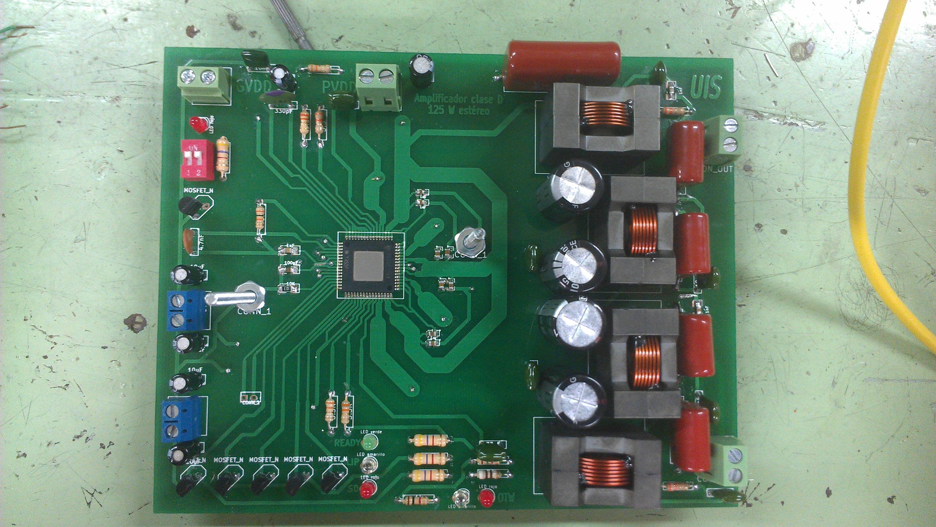
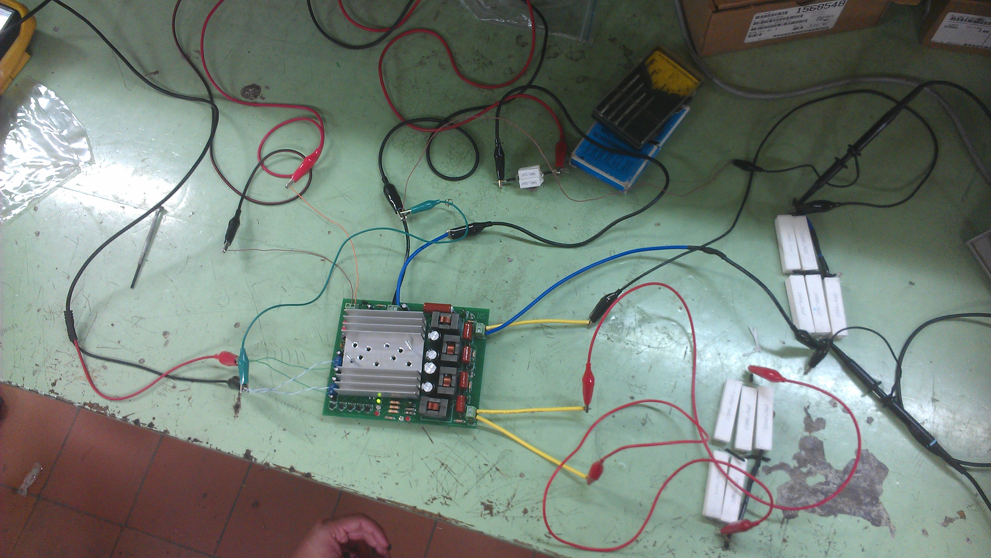
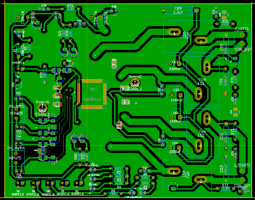
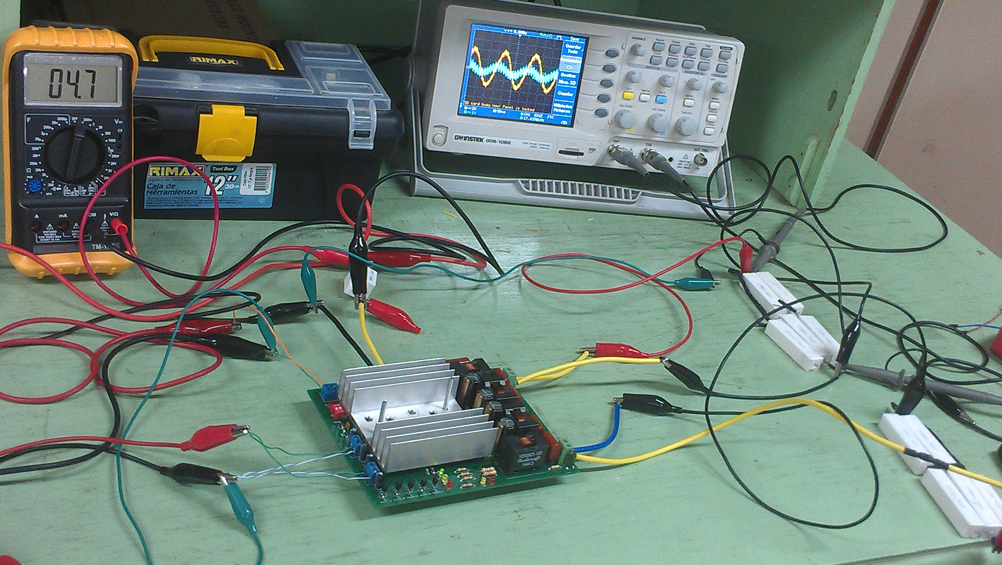
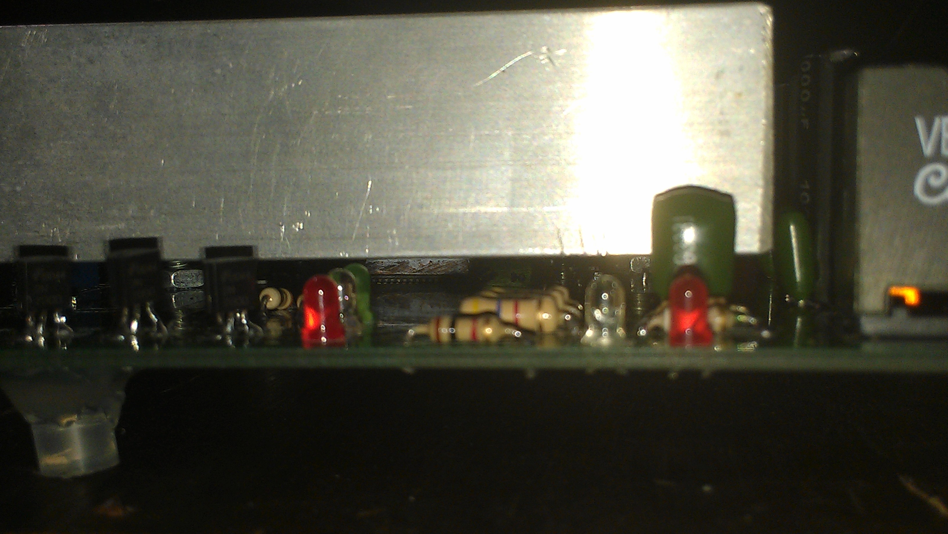
I make work a free sample of TAS5611a on my own PCB in BTL mode, I need to test the efficiency, then I use as a input signal a sinusoidal signal 1kHz of frequency, the same signal for each input, each output is conected to a load of 3.9 ohms. 

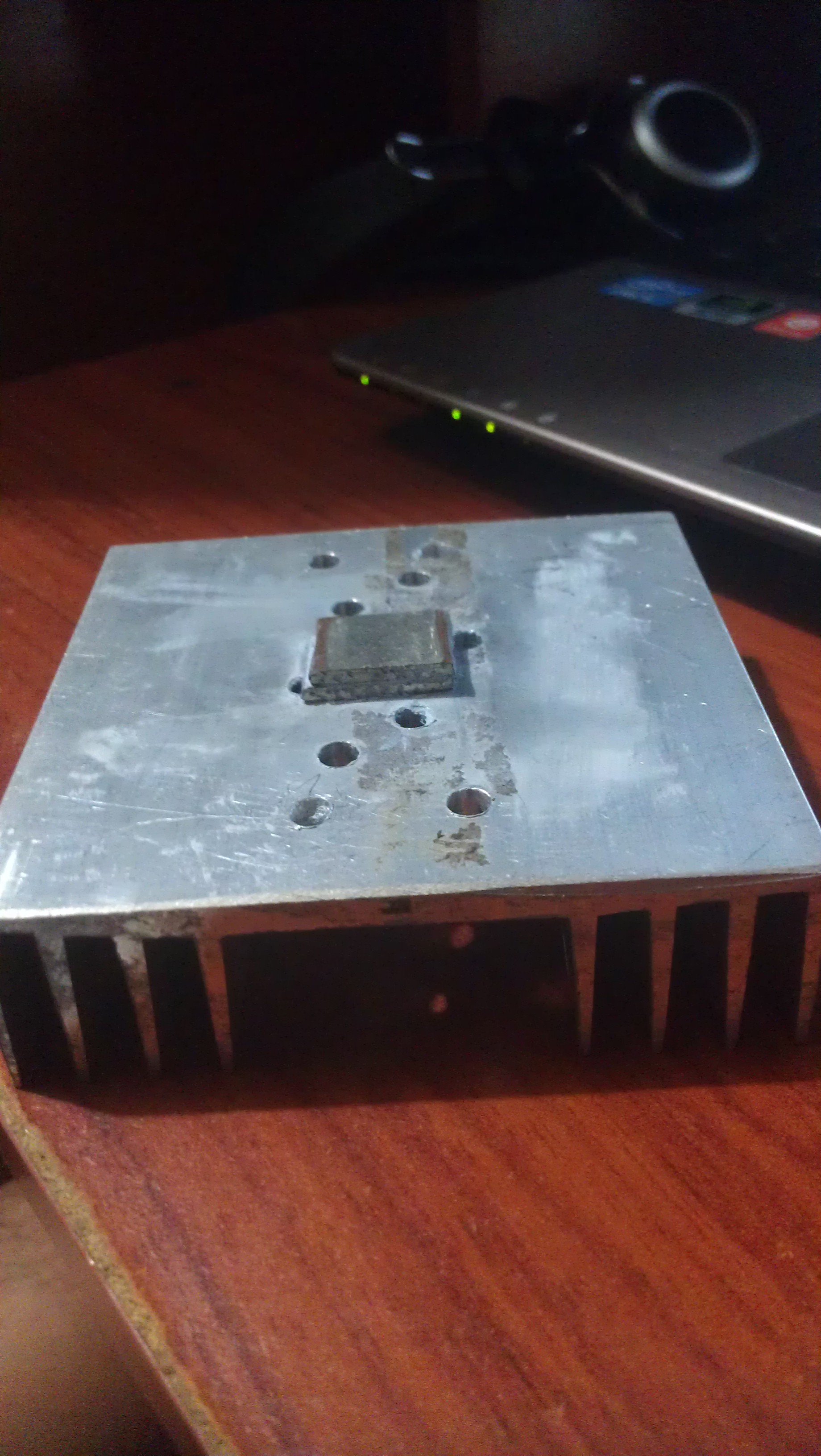
I increase the input signal then the output power increase, the problem is that I can´t increase de output power above 16 W without the chip get very hot, the signals OTW1 and OTW2 get activate when the output power is above 16W.

How I can get a output power higher?

thanks

  • Hi Andres,

    Sorry for telling you that, but your layout doesn't look good for me :( Do you have a single side PCB? The decoupling caps are way too far from the chip and the MLCCs look to small. Did you measure the temperature of the chip under 16W load? What is the real temperature. Did you connect any oscilloscope to see what is going on on the output playing 16W sine wave? Is the output signal distorted? Could you show the other side of the board?

    Why not to copy the reference layout available from TI?

    Cheers,
    Tomasz
  • Hi Tomasz

    Thanks for reply.

    the PCB is like that:

    The MLCC are as close as is posible, and the chip works. I didn't measure the temperature at 16 W, but the signals OTW1 and OTW2 are activated when the amplifier is working at 16W a little time (15 seconds perhaps), then I assume the temperature reach 125 °C, because the amplifier get reset when the OTW2 y activated.

    I connect a oscilloscope and saw the signals, the signals aren't distort at 16 W, just the chip gets hotter until reach 125°C.

    the amplifier works well, the two inputs are connected to the same signal (from signals generator), one pin is ground and the other is the sine signal. the output is one pin is the signal amplified to 20 dB and the other is a noise signal with 16 V of DC.

    I selected the elements for the PCB guided of the EVM.

    the reference layout available from TI where it is, it is in the datasheet?

  • Hi, Andres,

    How is the heat sink and the thermal interface material used? There is good heat transfer from the device to the heat sink? Does the heat sink get hot?

    reg,
    Paul.
  • I used the TAS5630 reference board layout doing my layout for TAS5630/TAS5615 and never faced any thermal problems. How is your heat sink connected to the thermal pad? Are you using any thermal grease?
  • Hi Paul and Tomasz

    thanks for reply

    I use a heat sink conventional, I think is of aluminio, also I use other pieces of the same material of the heat sink for touching only the IC. 

    The dissipator gets hot, but no much like the dissipator. I use gray paste dissipative.

  • Hi, Andres,

    I suggest trying arctic silver ceramique 2. We've used this with good result.

    www.arcticsilver.com/cmq2.html

    reg,
    Paul.
  • Hi Paul

    Thanks for reply

    I use a cream heat conductive, I think the problem is not so much the heat transfer, but the entrance I'm using.

    I do not use differential signals, but a simple ended signal from a signal generator. ie input pin is connected to ground and the other to the positive signal generator.

    one day the amplifier entered permanent state of reset, because I no connect to ground the input signal (single ended).

    Andres Pinto