This thread has been locked.

If you have a related question, please click the "Ask a related question" button in the top right corner. The newly created question will be automatically linked to this question.

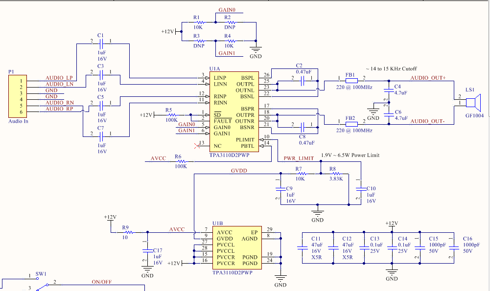
TPA3110D2 Constant Fault Tripping SD - Is this GAIN setting too high and creating too much DC Offset ? (PBTL Configuration)

Dear TI,

I have the design below and on power up (no input applied to any speaker audio input channels) the #FAULT Pin pulls low, cycles back to 2V, pulls low again, etc.  (BTW produces a series of low frequency click sounds on the speaker output at the same frequency as the shutdown fault cycle).

What would cause this ? Also occurs when I take the speaker off completely.  

Is the GAIN0 and GAIN1 settings too high ?  Also the PWR_LIMIT Voltage is 1.9V for a 6.5W limit and AVCC and GVDD all look clean and stable.

I checked with the PCB assembly house and they indicated that they made sure that the PGND pads for the heatsink were all properly attached etc.

I checked the temperature of the device and it is around room temperature so there is no thermal issue.

  • Hi Michael,

    Welcome to E2E and thank you for your interest in our products!

    I have a couple of questions about your application:
    - I see that you are using the amplifier in PBTL mode but why does LINN and LINP are not connected to ground ?
    - Is my understanding correct that the amplifier is recovering automatically from Fault?

    If the amplifier is able to recover automatically then it couldn't be a DC detection.

    I would suggest you to connect directly to ground LINN and LINP pins.
    Also it is recommended to hold /SD pin low at power-up to avoid faults due to the DC detect circuit.

    Best regards,
    Iván Salazar
    Texas Instruments
  • Hi Ivan,
    thank you for your answer. I tied LINN,LINP, RINN to ground through the AC caps as suggested in the EVM schematic. That did not change the
    behavior.

    Are you recommended adding cap to the SD & FAULT Node to have it pulled low while +12V ramps up ? That was not suggested in the app notes or datasheets. Also I tried tying the GAIN0 and GAIN1 to GND for minimum amplification and that did not help either.

    Anymore ideas :-)
    Thanks,
    Mike
  • Hi Michael,

    Another thing that you can try is to measure the auto-recovery restart time, it should be ~450mS. If this restart time is different then the problem could be at the +12V signal. You can also try by disconnecting /SD and /Fault to see if it is auto-recovering or going in and out of shutdown externally. This is not very common but could be an option.
    Also a decoupling capacitor in SD/Fault as you suggested is an option you can try in order provide a steady signal.

    Best regards,
    Iván Salazar
    Texas Instruments
  • Hi Ivan,

    Thank you again for your advice.  The recovery time is in the range of ~500ms you mentioned BUT you mentioned checking the +12V rail. I did a primitive check on the +12V only. So my next step is to trigger an oscope off the FAULT/SD signal and capture the +12V rail and see if there is any rail collapse or AC noise > +/- 160mv on the rail.  

    Also I wired in a DC Bench Top supply to eliminate the boost converter as a problem source.  The problem persists exactly the same with the DC Bench Supply.

    Another possibility is that there is a manufacturing defect in the PCB ? Anyway Ivan is there more information I can provide you ? Besides schematics, could you use layout ? etc.  This problem is holding up production on our commercial product.

    Thanks,

    Mike

  • Hi Mike,

    I can review the layout if you post it or send it to me.
    Another thing you can try is to remove the output filter by desoldering FB1 and FB2 to see if there's any problem at the output stage.

    Is this issue present in more than one board?
    Have you tried replacing the amplifier in your board?

    Best regards,
    Iván Salazar
    Texas Instruments