This thread has been locked.

If you have a related question, please click the "Ask a related question" button in the top right corner. The newly created question will be automatically linked to this question.

TPA3132D2 - Can leaving the input low damage the amplifier in single ended input mode?

Other Parts Discussed in Thread: TPA3132D2, DAC101S101, TPS62133

I've got your TPA3132D2 amplifier on a board I designed, powered by 12V, and I noticed that if the board had not yet been programmed to update the DAC which is providing audio input to the amplifier, the amplifier would get hot even when no speakers are connected.

I also just had a board with the amplifier die on me while testing another module but not updating the DAC.  The amplifier was hot when it died, and gets hot when I plug the power in.

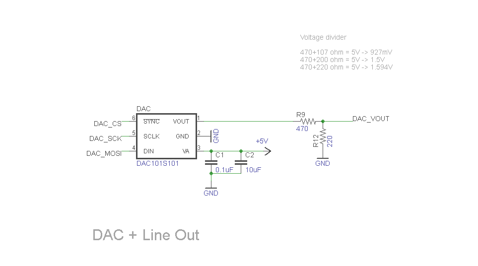
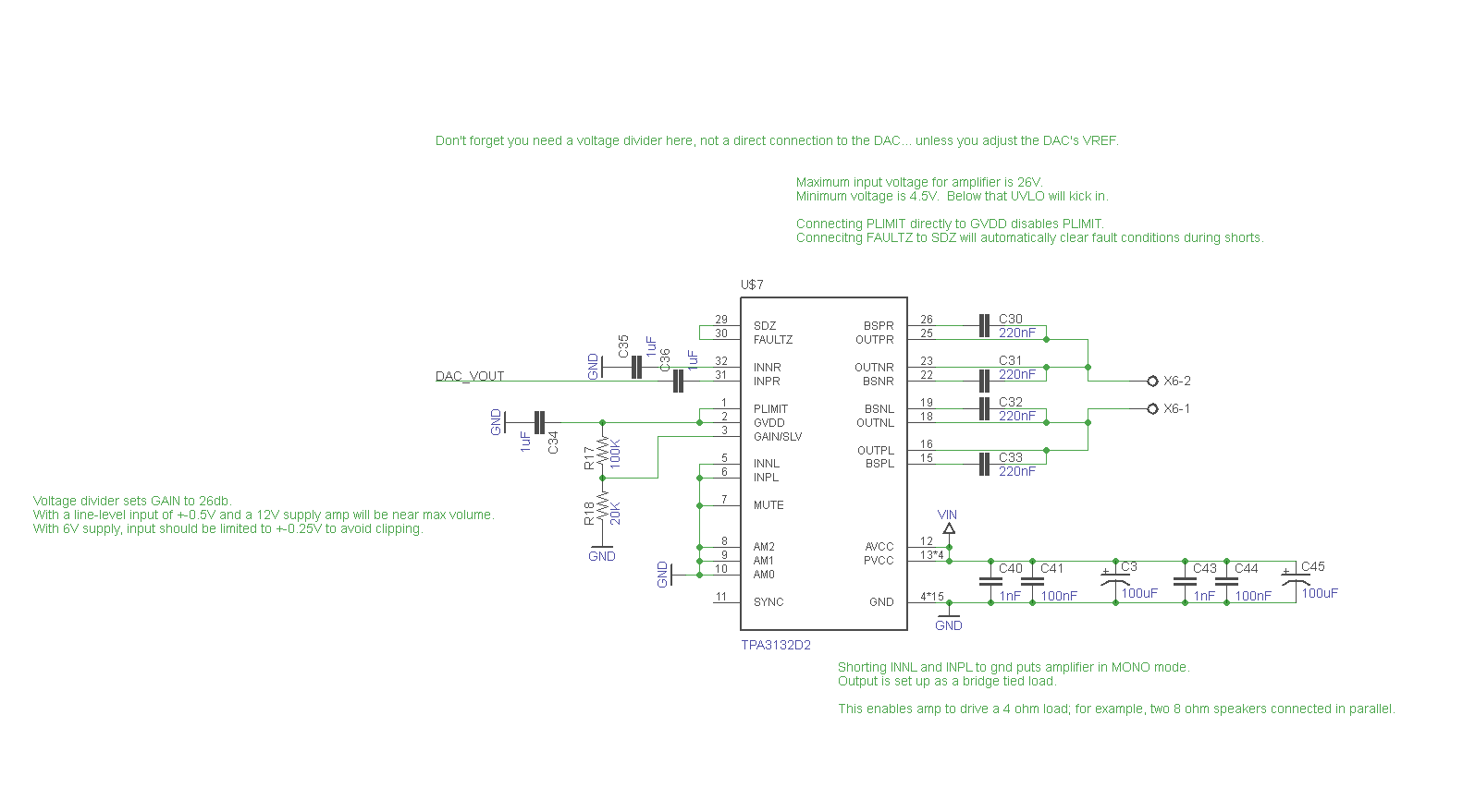
The amplifier is configured for PBTL with a sngle-ended input.  I have ceramic capacitors on INNR and INPR,with INNR's cap going to ground, and INPR's cap going to the DAC output, and INNL and INPL are shorted to ground.


Could it be that if the DAC is outputting 0V constantly because I am not sending audio to it, that this damaged the amplifier? 

The amplifier was working fine when I was testing audio.  It's just when no audio is being output to it (and no speakers connected) that there seems to be a problem.

  • Also please let me know how to resolve this. I am using your dac101s101, which defaults to GND on the output when powered up, and I have the SDZ pin wired to FaultZ for automatic recovery from faults. Should I connect MUTE to a pull up resistor and my microcontroller and pull it down only when I have configured the DAC and begun outputting audio? It is currently pulled to ground at all times.
  • Hi Shawn,

    Can you specify the application?
    Do you have a schematic you can share?

    The DAC101S101 appears to be a positive only voltage output DAC. That is the output only swings from ground to the rail. Therefore any audio will not be symmetric around ground. Not sure if this is the issue since the input blocking caps should take care of DC offsets.

    Do you have any scope shots of the PWM switching waveform from both the left and right PBTL output legs to ground before the LC filter and at the load with the DAC not configured?

    If your have a differential probe or your scope has a subtraction math function, can you also show the differential voltage before and after the LC filter?

    Do you have a scope shot of the output of the DAC before it is configured?

    Best Regards,
    Matt Beardsworth
  • Here are the relevant portions of my schematic:

    "Do you have any scope shots of the PWM switching waveform from both the left and right PBTL output legs to ground before the LC filter and at the load with the DAC not configured?"

    "Do you have a scope shot of the output of the DAC before it is configured?"

    No, I don't have a scope to check it out with.

    As you can see I followed the reference circuit for a single ended input almost to the letter, removing only some filters on the output that the datasheet indicated weren't absolutely necessary.

    What I believe is happening is when I power up the DAC it defaults to 0V.  This pulls the input capacitor down, the amp sees -1/2dacVout which in this case would be -0.8V, and this causes it to turn on the internal FETs that pull one side of the speaker down an pull the other side up.  And for some reason, in this state, even though no speaker is connected, large currents are being drawn.

    Here is the layout of the board that blew up, in case that helps:


    I've since revised the design like so, but I haven't yet had this manufactured.  Changes to the layout include a couple low ESR 470uF caps (the original design used generic 100uF caps, if that matters?  I assumed it would only potentially make the output noisier or make them heat up... and they did seem to heat a bit but that could have been them wicking heat from the amp), moving the DAC into the audio portion of the board and giving it a linear supply - your LP2980 5V regulator, as recommended in the DAC's datasheet.

    As for the application, this is a board which is designed to add lights, sound, and motion to costume props.  I added the linear regulator to the DAC to try to isolate any noise the servos and LED drivers might introduce into the circuit.  You can see one of your switching regulators, the TPS62133 next to the DC jack.  That supplies power to the rest of the circuit.

  • Hi Shawn,

    Without a scope this will be very difficult to debug.

    First thing that jumps out at me is R9 and R12. This is a very heavy load for the DAC and should be 10x to 100x larger. The R9 and R12 resistors will be pulling a lot of current to ground from the DAC.

    However, for debugging you should remove these all together.

    If you have a multimeter you can also check to make sure the DC voltage on the pin side of the input blocking caps are at the same bias voltage for the TPA3132D2. If not, the amplifier will be trying to amplify this DC voltage. The inputs should both be biased at 3VDC.

    Regards,
    Matt
  • I'm reading 2.96V with one probe on ground and the other on the pin side of each of those caps. This is with a second still working board.

    I have also verified that the DAC side is at 0V on startup.

    I will adjust the size of those resistors on the next board revision.