Team,
Customer of mine connects and configure an electret mike as per attached and doesnt get proper function. I checked Hw and it looks good. SW configuration looks ok as per comments but I didnt get into actual register checks.
Can you please advise or provide a reference configuration for electret mike?
static const unsigned char codec_conf[] =
{
///////////////// Initialization //////////////////
// Px, P0 Switch to Page 0
0x00, 0x00,
// s/w reset
0x01, 0x01,
//========== DIGITAL CONFIGURATION ==============
//===============================================
//---------- CLOCK Generation & PLL -----------
//------------------------------------------------
// Clock Setting Register 1 - Multiplexers
// -> PLL_CLK = (PLL_CLKIN x R x J.D)/P
// - PLL_CLKIN = PCM_Fs x XX
// -> 81.920MHz = (1.024MHz x 2 x 40.0)/1 --> For Fs = 32.0KHz
// P0, R4, b3-2. PLL_CLKIN = BCLK (01)
// P0, R4, b1-0. CODEC_CLKIN = PLL_CLK (11)
0x04, 0x07,
// Clock Setting Register 2 - PLL P and R Values
// P0, R5, b7. PLL = Power Up (1)
// P0, R5, b6-4. PLL Divider P = 1 (001)
// P0, R5, b3-0. PLL Divider R = 2 (0010)
0x05, 0x92,
// Clock Setting Register 3 - PLL J Value
// P0, R6, b5-0. PLL Divider J = 40 (101000)
0x06, 0x28,
// Clock Setting Register 4 - PLL D Value
// P0, R7, b5-0. (MSB) PLL Divider D = 0
// P0, R8, b7-0. (LSB)
0x07, 0x00,
0x08, 0x00,
// Clock Setting Register 18 - NDAC Values
// P0, R18, b7. NDAC = Power Up
// P0, R18, b6-0. NDAC = 4 (DAC_CLK = CODEC_CLKIN / NDAC)
0x12, 0x84,
// Clock Setting Register 19 - MDAC Values
// P0, R19, b7. MDAC = Power Up
// P0, R19, b6-0. MDAC = 5 (DAC_MOD_CLK = DAC_CLK / MDAC)
0x13, 0x85,
// DAC Setting Register 1 - AOSR Value
// -> ADC_Fs = CODEC_CLK_IN / (NDAC.MDAC.AOSR)
// -> 32.0KHz = 81.920MHz / (4.5.128)
// -> MDAC * AOSR >= ResourceClass * 32
// - 5 * 128 >= 8 * 32 (256)
// -> 2.8MHz < AOSR x ADC_Fs < 6.2MHz
// - 128 * 32000 = 4.096MHz
// -> AOSR must be a multiple of 8 (48KHz High-Performance)
// -> AOSR = 64, for Low-Power Mode
// -> AOSR = 128, for High-Performance Mode
// P0, R20, b7-0 AOSR = 128 (ADC_Fs = ADC_MOD_CLK / AOSR)
0x14, 0x80,
// ADC => NDAC is powered up and set to 4
// Clock Setting Register 18 - NDAC Values
// P0, R18, b7. NDAC = Power Up
// P0, R18, b6-0. NDAC = 4 (DAC_CLK = CODEC_CLKIN / NDAC)
0x0b, 0x84,
// MDAC is powered up and set to 5
// Clock Setting Register 19 - MDAC Values
// P0, R19, b7. MDAC = Power Up
// P0, R19, b6-0. MDAC = 5 (DAC_MOD_CLK = DAC_CLK / MDAC)
0x0C, 0x85,
// DOSR = 128, DOSR(9:8) = 0
0x0D, 0x00,
// DOSR(7:0) = 128
0x0E, 0x80,
//---------- Digital Interface Settings -----------------
//---------------------------------------------------------
//Mode is DSP mode,wordlength is 16
//=> P0, R27, b7-6. Interface Mode = DSP Mode (01)
//=> P0, R27, b5-4. Data Length = 16bits (00)
//=> P0, R27, b3. BCLK = Input (0)
//=> P0, R27, b2. WCLK = Input (0)
0x1b, 0x40,
// Data offset is 1 BTCLK
//=> P0, R28, b7-0. Data Offset = 1
0x1C, 0x01,
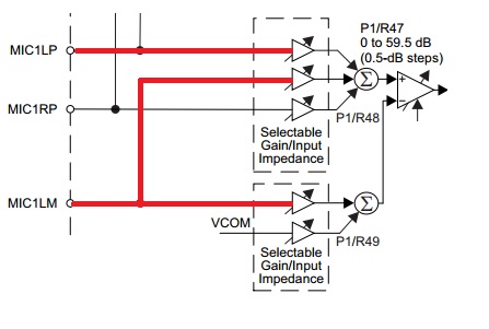
//================= MIC COnfiguration =====================
//==========================================================
//------------------ page 1 is selected
0x00, 0x01,
// MICBIAS Control Register
// P1, R46, b3 Programmed MICBIAS is powered up even if headset is not inserted (1)
// P1, R46, b1-0 MICBIAS output is powered 2.5V (10)
0x2e, 0x0a,
// MICPGA P = MIC 10k
//0x30, 0x40,
//0x30, 0xC0, //Before electre
0x30, 0x44, //MIC1LM connected
//0x30, 0x80,
// MICPGA M - CM 10k
//0x31, 0x40,
//0x31, 0xC0, //Before Electre
0x31, 0x10,
//P1, R47, MIC PGA
//0x2F, 0x14, //1E => 15 db - 0x14 - 10DB
//P1 register 50 - electre
0x32, 0x20,
//===============================================
//========== ADC / DAC Data Pathes ==============
//===============================================
//-------- page 0 is selected
0x00, 0x00,
//-------- ADC Data Path ----------------------
//POWERUP ADC Digital MIC channel
//=> P0, R81, D7. ADC channel = Powered up (1)
//=> P0, R81, D3. Digital microphone is enabled for delta sigma mono channel = (1)
//=> P0, R81, D1-D0. Soft Stepping control = enabled (01) 1 step / 2 sample period
0x51, 0x80,
// UNMUTE ADC channel - ADC Digital volume control fine adjust
//=> P0, R82, D7. ADC channel = Not Muted (0)
//=> P0, R82, D6-D4. DeltaSigma Mono-ADC channel fine Gain = 0dB (000)
//=> P0, R82, D3-D0. reserved wite 0 these bits
0x52, 0x00,
//P0, R83 ADC Digital Volume Control Coarse Adjust
0x53, 0x28,
//-------- DAC Data Path ---------------------
//Power UP DAC_DATA_PATH_SETUP(D7=1), Left Channel data path = left data (01), period stepping (00) 1 step / sample
//=> P0, R63, D7. Left Channel DAC = Powered up (1)
//=> P0, R63, D6. Right Channel DAC = Powered Down (0)
//=> P0, R63, D5-D4. Left Channel DAC data path = left data (01)
//=> P0, R63, D5-D4. Right Channel DAC data path = left data (01)
//=> P0, R63, D1-D0. Soft Stepping control = enabled (00) for 1 step / sample period
0x3F, 0x90,
//-------- DAC Volume CTRL ---------------------
//=> P0, R64, D7-D4. Reserved = (0000)
//=> P0, R64, D3. Left Channel DAC = Not Muted (0)
//=> P0, R64, D2. Right Channel DAC = Not Muted (1)
//=> P0, R64, D1-D0. Left & Right independant Volume control (00)
0x40, 0x04,
//P0, R65, DAC_left_volume_control => 12 dB gain left
//0x41, 0xf8,
//0x41, 0x18, //12db
0x41, 0x30,
//-------- DAC Instruction Set ---------------------
//=> P0, R60, D7-D5. Reserved = (000)
//=> P0, R64, D4-D0. DAC Signal Processing Bloc pRB_B5 (0 1001)
0x3c, 0x05,
//-------- SPL Class-D / Analog Attenuation ------
//--------------------------------------------
//---------------- Select Page 1
0x00, 0x01,
//Class-D_Drivers Setup
//=> P1/R32, D7 Left Class D driver = Power Up (1)
//=> P1/R32, D6 Right Class D driver = Power Down (0)
//=> P1/R32, D5-D1 Reserved = Reset Value (00 011)
//=> P1/R32, D0 Read Flag= Short circuit detected on the Class-D driver
0x20, 0x86,
//SPL/MIX_L Analog Amplifier Attenuation
//=> P1, R38, set to 1000 0000 OdB
//0x26, 0x80,
0x26, 0x00,
//SPL/Class-D Speaker Driver
//=> P1, R42, D7-D5 (000) reserved and set 0
//=> P1, R42, D4-D3 (11) Left channel class-D output stage gain is 24dB
//=> P1, R42, D2 (1) Left channel Class-D is Not Muted
//0x2A, 0x0C, //12db
//0x2A, 0x14, //18db
0x2A, 0x1C, //24db
//-------- HPL Class-A/B driver / Analog Attenuation ------
//---------------------------------------------------------
//HPL/MIX_L Analog Amplifier Attenuation
//=> P1, R36, set to 1000 0000 OdB
0x24, 0x80,
//HPL/Class-A/B Headphone/Lineout Driver
//=> P1, R40, D6-D3 (0000) HPL driver PGA = 0dB
//=> P1, R40, D2 (1) HPL drvier is not muted
//=> P1, R40, D1 (1) HPL drvier is high impedance in Power down
0x28, 0x06,
//Routing LDAC and RDAC output to SPK_LP
//=> P1, R35, D7-D6 DAC_L is routed to the left channel miser amplifier = (01)
0x23, 0x40, //Before electre
0x23, 0x60,
//===================================
//========== DRC Setup ==============
//===================================
// Select Page 0
0x00, 0x00,
//DRC Enabled
//=> P0, R68, D6-D5, DRC enabled
//=> P0, R68, D4-D2, DRC Threshold value =
//=> P0, R68, D1-D0, DRC Hysteresis value =
//P0, R68, DAC => DRC enabled for both channels, Threshold = - 24dB, Hysteresis = 3 dB
0x44, 0x57,
//P0, R65, DAC_left_volume_control => 12 dB gain left
0x41, 0xe0,
//P0, R69, DRC Hold = 0 ms, Rate of changes of gain = 0.5dB/Fs
0x45, 0x00,
//P0, R70, Attack rate = 1.9531e-4 dB/Frame, DRC Decay Rate =2.4414e-5 dB/Frame
0x46, 0xb6
};

Thanks