This thread has been locked.

If you have a related question, please click the "Ask a related question" button in the top right corner. The newly created question will be automatically linked to this question.

Having problems with input data stream on TLV320AIC34.

Other Parts Discussed in Thread: MSP430F5359, TLV320AIC34

Hello,

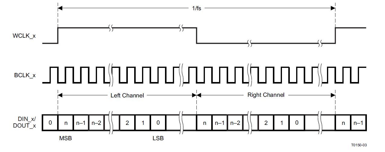
As I've posted before, we've implemented a new hardware design that uses the TLV320AIC34 connected to an MSP430F5359 using the connections described in app note is based on the appnote SLAA449A.  We're running the MSP430 at 20MHz and supplying that 20MHz clock to the Codec's MCLK_A & MCLK_B inputs.  I'm attempting to sample a signal around the 20Khz range in this example.  Here is my Codec Configuration sequence:

Start by resetting the Codec A & B.
Delay 5 microseconds
Release reset on Codec A & B.
Delay 10 microseconds

Set the following Registers to Configure
  Data stream and clock configuration:
Register   Addr    = Value
Register  7 (0x07) = 0x80
Register  9 (0x09) = 0xC0
Register  3 (0x03) = 0x21
Register  2 (0x02) = 0x22

Set Differential Input Register Configuration:
// Left Channel Config CodecA & B
Register   Addr    = Value
Register  7 (0x07) = 0x8A
Register 43 (0x2B) = 0x00
Register 37 (0x25) = 0xC0
Register 82 (0x52) = 0x80
Register 86 (0x56) = 0x09
Register 40 (0x28) = 0x40

// Right Channel Config CodecA & B
Register   Addr    = Value
Register  7 (0x07) = 0x8A
Register 44 (0x2C) = 0x00
Register 37 (0x25) = 0xC0
Register 92 (0x5C) = 0x80
Register 93 (0x5D) = 0x09
Register 40 (0x28) = 0x40

I have previously configured the SPI interface to use a bit rate divider of 0x1F which should yield a real divider of 0x20, or 32.  My input clock to the SPI peripheral should be the SMCLK for the micro which is the same clock being fed to the codec's MCLK.  This clock should be set at something close to 20Mhz.  So, my bit rate on the SPI interface should be 20Mhz / 32 = 625Khz.

So, the "sampling frequency", or the frequency that I should be reading samples out of the codec should be 625khz / 32 bits = 19531.25.

The corresponding setting based on my codec configuration should be setting fsref as 20Mhz / (128/Q) where Q = 4 which yields a value of 39062.5.  I then have the ADC/DAC sampling set to fs/2 which yields the final sampling frequency of 19531.25 which should be an EXACT match to my SPI sampling frequency.  Especially when we consider that both the codec and my SPI port are clocked with the same 20Mhz clock source.  Things should be synchronized.

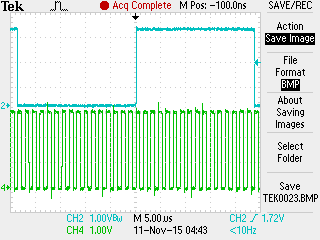
However, in my input data stream that I read from the codec, I can see "flat spots" in my input sine wave periodically occurring once every 32 samples.  I have no explanation for this.  My SPI ports are all DMA driven so interrupt latency should not be an issue.  By DMA sample size is currently set to 64 samples, so even that doesn't correspond to the precise 32 sample flat spots.  It sure looks like I'm getting out of sync with the codec somehow, but I cannot see where this could be happening.

Attached is an excel spreadsheet showing the data sampled from the codec.  I have some initial startup sync issues in my buffer, so the first 60 or so samples should be ignored.  However, following that, you can clearly see how the flat spots occur regularly at 32 sample intervals.

TestDataStream.xlsx

  • Hi, Christopher,

    I think it could be related with the BCLK and WCLK (LRCLK) frequencies. I understand that you're configuring the WCLK as 19531.25 Hz (as the sample frequency). What about the BCLK frequency? It must be at least calculated as BCLK = WCLK * # of channels * # bits.

    Best regards,
    Luis Fernando Rodríguez S.
  • Hi Luis,

    I guess I wasn't clear enough.  The BCLK is the SPI Clk.  This is what is done in the SLAA449A app note that I mentioned.  That app note calls out extra circuitry between the MSP430 and the codec to transform the SPI signals into the "Left Justified" format used by the codec.  As I mentioned, the SPI clock rate is set to 625Khz.  Since there are 32 bits (16 bits left, 16 bits right) in each sample, dividing 625Khz by 32 yields the 19531.25 hz.

    So, the clocks should be in perfect sync especially since both the SPI peripheral in the MSP430 and the Codec are both using the same 20mhz clock input.

    So you have any other ideas as to what may be causing the synchronization issue?  I'm running out of ideas.

    Thanks,

    Chris.

  • Hi, Chris,

    I apologize for the late response.

    I have been checking your register configuration and the SLAA449A app note. It seems that your clock configuration is in order. However, I suspect that the input data is wrong. Each 32 samples, a value is repeated. How are you generating the input data? Could you check it, please?

    Thank you.

    Best regards,
    Luis Fernando Rodríguez S.
  • Hi Luis,

    I am not entirely sure what you are asking me here. The spreadsheet I supplied, where "Each 32 samples, a value is repeated" is the data I read from the codec. It isn't "input data". I am using a signal generator to generate a 1khz sine wave input to the codec. I then start the codec sampling operation. The data values I sampled are placed in a buffer in memory in my MSP430. I then use my debugger to dump that memory buffer and then import that data into excel. This is the data you see in the spreadsheet. As you can see, once every 32 samples, a value is duplicated. This implies to me that for some reason, the codec outputs the same value on two consecutive samples. As I've been told, and observed in the past, this is generally indicative of a clock synchronization issue. I just don't understand where the synchronization issue could be given the setup of the SPI interface and the Codec clocks as I've previously documented above.

    To me it almost seems like the codec is either dropping or gaining one bit clock for every sample. This would cause my sample to drift off one complete sample every 32 samples which in turn would cause the duplicated data sample. I just don't see how this could be happening.

    Chris.
  • Hi, Chris,

    I apologize for the confusion. After check your last information, I suspect that the problem could be related with the WCLK (LRCLK) generation. Every 32 samples, a value is duplicated. Probably this means that there are 33 bits per WCLK frame. This additional bit could be generating an additional value every 32 samples. Have you checked both clocks (BCLK and WCLK) with an oscilloscope? Have you checked if the number of pulses is correct?

    Best regards,
    Luis Fernando Rodríguez S.
  • Hi Luis,

    Yes, that is exactly what I checked.  I put my scope on BCLK and WCLK.  Here is what it looks like:

    By my count, it looks like exactly 32 BCLKs (Green) for the WCLK cycle (Blue).  16 bclks in each half of the WCLK.

    To my eye, this waveform seems to match exactly the waveforms described in the SLAA449A app note.

    Chris.

  • Hi, Chris,

    I have been checking your information with my colleagues of the audio team. First, we noticed that the BCLK and WCLK have some differences with the timing diagram of the datasheets. In left-justified mode, BCLK falling edge must match with the WCLK rising edge as the following picture shows:

    In the last picture that you sent us, it seems that your BCLK is inverted (both rising edges match). Could you try inverting the BCLK signal, please?

    Additionally, we noticed that you're using both channels to get samples. Could you try only with one channel to see it affects the result?

    Thank you.

    Best regards,
    Luis Fernando Rodríguez S.

  • Yes, I noticed that clock inversion / discrepancy before as well when comparing my trace with the tlv320aic34 datasheet for left justified mode.  However, the clocking matches EXACTLY the waveform that was published in the SLAA449A app note.  Specifically, in this snippet, you can see the WCLK changing synchronously with the rising edge of BCLK:

    I will work with my hardware designer to see if there is any way we can invert the clock.  I'm not entirely sure what you mean by "trying with one channel only".  Is there some specific Codec configuration you'd like me to try.  If so, could you please be specific as to the register configuration you'd like me to setup?  I don't want to get into a situation where I attempt to configure something that wasn't exactly what you wanted me to try.Thanks,

    Chris.

  • Hello,
    I've been considering your request to invert BCLK and it isn't clear to me exactly where you'd like the inversion to be made. Please refer to the SLAA449A app note circuit and it's connection to the MSP430's peripheral. There are things that can be done with the SPI Clock phase and polarity via MSP430 register manipulations to change the relationship of the clock edges and how data is presented or sampled on the interface. If you could possibly describe in detail how and where you would like the inversion to be made, I could work with my hardware designer to manipulate circuit and/or I could modify the MSP430 register configuration. However, I need more to go on that just "Invert BCLK".
    Also, I find it troubling that in the TLV320AIC34 datasheet that the only waveform / timing diagram listed where the different modes (Left-Justified, Right-Justified, IIS, and DSP) that doesn't have "extra" bclks" between the Left and Right data is the DSP mode. All the other modes always seem to show additional BCLK clock cycles between the LSB of Left and MSB of Right channel data. I don't know if this was intentional, or if this was just they way the diagrams were drawn.

    Please let me know as soon as you can how and/where you'd like the BCLK inverted.
    Thanks,
    Chris.
  • Hi, Chris,

    We suggest to add an inverter between the SCLK output and the BCLK input as the following diagram shows:

    This connection will ensure that the BCLK will be inverted:

     I'm confusing about why this app note recommends to use the BCLK in that way. The Figure 1. I 2 S/LJF/RJF Timing in Master Mode specifies that the BCLK falling edge must match with the falling/rising edge of the WCLK. So, we expect that this test will improve your sampled signal. Is it possible for you to invert the BCLK in that way?

    Then, regarding the register configuration, it would be fine to try to use one channel at time. Is it possible to sample the signal only with the left channel? I mean, could you omit to use the following code lines:

    // Right Channel Config CodecA & B
    Register   Addr    = Value
    Register  7 (0x07) = 0x8A
    Register 44 (0x2C) = 0x00
    Register 37 (0x25) = 0xC0
    Register 92 (0x5C) = 0x80
    Register 93 (0x5D) = 0x09
    Register 40 (0x28) = 0x40

    Finally, regarding your comment about the DSP mode, that timing diagram was drawn in that way intentionally. The DSP mode start the data transfer with the left-channel data first and immediately followed by the right-channel data. So, that's why there are no BCLK clock cycles between the LSB of Left and MSB of Right channel data.

    Please let me know if you still have questions or comments.

    Best regards,
    Luis Fernando Rodríguez S.

  • Luis,
    What I meant when I asked about how the timing diagrams were drawn was that the DSP mode was the only drawing that showed continuous clock and data. All the others show the potential for additional, possibly unused, BCLKs between the left and right channel data. It is not clear to me if these additional BCLKs are actually required in the other modes. The DSP mode was the only one where the timing diagram showed a continuous flow of data from the left channel to the right channel and back to the left channel with now "gaps" or extra bclks.

    Do the other modes (Left justified mode for example) expect to have at least one or more BCLKs present between the channel data?
    Chris.
  • Hi, Chris,

    The other modes can have more BCLK between the channel data. However, these bits would be ignored. Let's see the following example:

    If WCLK = 44.1kHz, word length is 16-bits and there are 2 channels to be used, you should configure the BCLK as 2*16*WCLK (1.412 MHz). This configuration ensures that the codec will have 16 BCLK per WCLK frame (or per channel). However, the BCLK frequency can be higher and there would be no problem. Even with the same values, the BCLK could be configured as 2.8224 MHz. It means that there would be 32 BCLK per WCLK frame. However, if the codec is configured with a word length of 16-bits, the rest of the bits (16 per channel) will be ignored. (This is actually the clock configuration on the TLV320AIC34 EVM).

    Best regards,
    Luis Fernando Rodríguez S.

  • Hi, Chris,

    We already tested this issue on the TLV320AIC34EVM. We used an Audio Precision tool to generate the same clocks that you have. Then, we generated an 1kHz sine wave on the analog input. However, we observed that you register configuration is not complete. There's no ADC configuration on your register sequence.

    We configured the codec to get samples with the ADC. We observed that the sine wave is sampled correctly when the device is configured in differential mode.

    How did you configure the TLV320AIC34 to get samples? Could you provide the ADC register configuration, please?

    Best regards,
    Luis Fernando Rodríguez S.
  • Hello Luis,


    Thank you for continuing to research this issue.  I too have been looking into things here.  We decided that since the SLAA449A app note seems to have problems with the waveforms and signal timings that we would pursue other solutions to connect the TLV320AIC34 to our MSP430F5359.  The DSP MODE looked promising.  I was able to come up with a method to connect the MSP430 to the codec without any external glue logic.  I simply ran the SPI Clock into one of the timer clock inputs on the MSP430 and used the timer output to generate the WCLK pulse at the appropriate time to implement the DSP MODE serial interface.

    After I wired this up, I was still seeing the flat-line once every 32 samples.  The only explanation I had for this, which is the same explanation you've had all along, is that the sampling frequencies are not matched.  I could not understand how this could be given that both the SPI and Codec are both clocked from the same clock signal and were theoretically configured to generate identical sampling rates.

    Well, it turns out that there was a bug in the MSP430 data sheet.  I was using SLAU208N, since at the start of this project, that was the current datasheet for the MSP430x5xx family of CPUs.  In that datasheet the bit rate clock for the SPI was defined as BitClk = BRClk / (UCBRx+1).  So in my calculation, the BitClk = 20Mhz / (31+1) which comes out to 625khz.  A 625khz bit clock would match the Codec sampling frequency EXACTLY.  It turns out that there is a new datasheet for the MSP430x5xx family, SLAU208O.  In that datasheet, the bitclock equation is BitClk = BRClk / (UCBRx).  Note the "+1" was dropped!!!  So, in my testing, my bit clock was actually being configured 1/32 too fast.  This would mean that once every 32 samples, I would "double read" the same sample thereby giving me that flat-line.

    I believe this is the root cause of my problem.  The datasheet was wrong!  I have made the appropriate changes to my code and will test it soon.  I will let you know what I find out, but I am optimistic that this will solve the flat-line issue I was seeing.

    This was a good exercise anyway.  It resulted in us being a able to simplify the hardware design and remove all that extra glue logic that was required to generate the "left-justified" signal from the SPI signal.  And, as you and your colleagues determined, the SLAA449A Left Justified mode operation was not exactly correct anyway since it failed to properly maintain the correct clock polarity with respect the the WCLK_x signal.  The current implementation will require I use two timer resources in the MSP430 to generate the appropriate WCLK_A and WCLK_B pulses given the two SPI Clock sources.  This will be a much cleaner design in the end.

    I would highly recommend that you take down the SLAA449A app note and either re-write it to included your proposed hardware modification that included the extra inverter or, you do something like I did and use DSP-MODE with MSP430 timers so generate the WCLK_x signals.

    Again, thanks for your help so far and I will let you know how my next round of testing goes with DSP-MODE.

    Chris.

  • Hi, Chris,

    Thank you for the feedback. I agree with you, it seems to be the root cause of this issue. We will be waiting for the results to be sure that it fix the problem.

    I already talked with my colleague about the SLAA449A app note. We are going to update the information to avoid the future problems related with it. I apologize for the confusion that it caused.

    If you still have questions or comments, please let me know.

    Best regards,
    Luis Fernando Rodríguez S.