This thread has been locked.

If you have a related question, please click the "Ask a related question" button in the top right corner. The newly created question will be automatically linked to this question.

PCM1794 mono mode left right

Other Parts Discussed in Thread: PCM1794, PCM1794A

Hello,

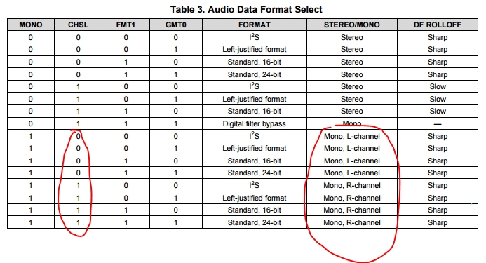
I want to use the PCM1794 in mono mode with 2 PCM1794. I understand that I have to delay the signal of 7 bits + 32 bits to align the two signals for the two dacs.

see: e2e.ti.com/.../250826

How do the converter know that it has to decod only the left or the right part of the signal ? Does it decod everything it get  in the DATA pin ?

If yes, does it mean I have to split completely the signal in two parts one part only right, the other only left and to align both ?

Best regards,

Michel

  • Hi Michel,

    When in mono mode, the part will look at the data content that is specified for the mode. These modes are explained in Table 2, and shows that the PCM1794A supports I2S, left justified, and right justified ion mono or stereo.

    I'm not sure why you have to delay the signal, can you explain that more? If its about when the DACs will output, they will output at the end of EACH LRCK frame, which means after both channels content has been transmitted.

    Justin
  • Hi Michel,

    You need 7 bit data delay and 32 bit left-channel buffer. You will get two simultaneous data signals converted to right-justified format. Simple solution is to use 5x 74HCT164 chips. Similar circuit created Doede Douma: http://www.dddac.com/dddac1794_design.html

    Best regards,

    Pavel

  • I am having trouble understanding why the delay is needed. If the PCM1794A can be told which channel to use in mono mode(L or R), as well at what format, and will wait until both channels are received before latching to the output, then no delay should be needed.

    Is this a question of the format and how to modify it?

    Justin
  • Hi,

    If I use a CS8416, I will have a signal left/right in right justified mode. I would like to use the PCM1794 in mono mode in order to deactivate the digital filter. 

    Thus, I understand that I have to split the signal in left for the first PCM1794, then right for the second PCM1794. PCM1794 in mono mode will latch the signal during a period of LRCK. So I have to be sure that during a period of LRCK I present to the first PCM1794 the left frame, and to the second PCM1794 the right frame.   Both must be synchronized. Is it right ?

    The delay is used to align right part and left part of the PCM signal. I read a previous answer that I have to delay the signal of 7 clock state and buffered the signal during 32 bits see: e2e.ti.com/.../250826. I try to do it with excel spreadsheet and for me it seems that it doesn't work 

    My question concerns the operation I have to do to modify the format. I'm a little bit lost.

    Best regards,

    dac-bits.xlsx

  • Hi Michel,

    You do not have to split the signal for left and right. The PCM1794A can take in both signals in left and right channels when in mono mode. You then control which channel the device will output. However it will still wait for both channels to be input before the analog output is changed. The example shown that you keep linking to is based off the PCM1704, which is not the same device, and has a different digital interface.

    Just to clarify in the PCM1794A data sheet, standard mode, is really right justified. So if this is the issue you are pointing to with the other E2E thread, then you do not need to modify the format, just use standard mode on the PCM1794A.

    Justin
  • Hello Justin,


    Thanks for your answer. You said 'The PCM1794A can take in both signals in left and right channels when in mono mode. You then control which channel the device will output.'

    How do I say to the PCM that it the right or left channel ? (because the channel select is used to desactivate the digital filter chapter 7.3.4)

    Best regards,

  • Hi Michel,

    When in stereo mode you are correct, the CHSEL pin selected the filter, but if you look at the lower half of  the table, you see that the CHSL pin selects L or R.

    Justin

  • Hi Justin,

    Thanks you for your answer. Your remark is right but the digital filter is not deactivated.

    If you look to the table, it says that to bypass the digital filter I have to put 

    MONO =0
    CHSL =1
    FMT1=1
    GMT0=1

    In this mode, I have to put the "good frame" right for PCM1794 #1 and left in PCM1794 #2 during one LRCK period at the same time. This is the reason of my question. 

    Best regards,

    Michel 

  • Hi Michel,

    Sorry I didn't realize you were trying to use this in external filter mode. To use this mode you will need to be inputting to the device at 4x or 8x the desired sampling rate. Now that this is clear the delay circuit makes sense.

    Justin
  • Hi Justin, I thought MONO mode with "internal DF Bypass mode". In the datasheet on page 24 you can see, that in this mode is used right-justified mode with data only for one channel. 7 bit delay is needed for conversion of data from I2S mode. 32 bit buffer is needed for buffering of data for left-channel. It is because is needed to latch data on the audio outputs simultaneously.

    You can use simple glue logic without buffer, but with simple invertor on LRCK (WDCK) signal on one channel. Disadvantage of this solution is that channels are not played simultaneously but alternately.

    For MONO modes which use internal digital filter you don't need any logic, because in these modes DAC accept standard DATA formats and channel is selected with CHSL pin.