This thread has been locked.

If you have a related question, please click the "Ask a related question" button in the top right corner. The newly created question will be automatically linked to this question.

Regarding ADC PCM1860-full scale input range

Other Parts Discussed in Thread: PCM1860, PCM1862

Hi There,

We are planning to use PCM1860 ADC with electret condensor microphone (WM-64C) with sensitivity of -45dB for our application.

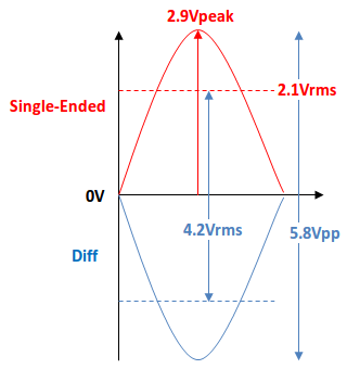
So microphone will generate output voltages in the range of around 5.6mV. But in the PCM1860 chip, it is specified that 2.1Vrms is full scale input voltage for single ended input.

my questions are 

1) whether this 2.1Vrms is the ADC input voltage range (after PGA in the chip) or it is the maximum input that i can give at the input pins VINR/VINL

2) Since PCM1860 operates at single power supply of 3.3V, how we can give 2.1Vrms (around 5.6Vpp) to the chip?

3) Can i give microphone input in the range of millivolt directly to the ADC or do i  need to add external preamplifier before giving to ADC pin VINL/R? or can i use internal PGA to convert this millivolt range to 2.1Vrms? if so then this 2.1Vrms should be the input of ADC block in the chip. 

Please share your comments to proceed further with this chip selection.

Thanks &  Regards,

Murugan

  • Hi Murugan,

    1. 2.1 Vrms is the maximum voltage you can input into the part per input pin. So if operating in differential mode, using two input pins, the largest differential signal that could be input would be 4.2 Vrms.

    2. This is proprietary information that we use for our front end of this device.

    3. For the PCM1860, you have 0 dB, +12 dB and +32 dB PGA gain available on CH4 for Single Ended inputs. For differential inputs you have 12 dB PGA gain available on CH2. If you move to the software controlled parts, PCM1862 and up, you have more options ( digital PGA and also the Digital mixer can add gain). 32 dB will not get you to 2.1 Vrms from 5.6 mV so if you will need the external preamplifier.

    Justin
  • Hi Justin,

    Thanks for your inputs.

    Sorry, Still i am not understanding the point regarding PGA,

    1) If we need to give maximum input voltage range of 2.1Vrms and if we are giving 2.1Vrms as input by using external preamplifier then what is the use of internal PGA in this case?

    2) Eventhough we are giving 2.1Vrms as input to VINL/R pins and enable the PGA inside the chip then what will be the maximum input voltage range for ADC?

    3) Can i add the external preamplifier to convert the 5.6mV to 2.1Vrms before giving to the chip? in this case should i need to disable the PGA?

    Please clarify.

    Regards,

    Murugan

  • Hi Murugan,

    If you have an external preamplifier to boost the signal from 5.6 mV to 2.1 Vrms, then you can leave the internal PGA at 0 gain. The maximum input to the part of 2.1 Vrms is also full scale input to the ADC, when the internal PGA is set at 0 gain.

    Justin
  • Hi Murugan, Justin,

    Your discussion is really helpful for me to understand the input specification.
    Here I prepare quick drawing with regards to input swing specification.
    Please correct me, if I'm wrong.


    But I have another question. We have the absolute max specification in the datasheet as below.
    I'm concerned that if we have 4.2Vrms(5.9Vpp) swing, it seems out of specification.


    Thanks,
    Ken


  • Hi Ken !

    We are also working on a project based on this chip. And we are asking ourselves the same questions !

    We assume that Analog input are biased at Vref, i.e. 0.5xVCCA as stated in the datasheet. So 1.65V. This will mean that your sinus schematic should not be centered to 0, but +1.65V. It will lead to a positive swing of 5 - 1.65 = 3.35V, and a negative swing of -1.7 - 1.65 = 3.35V too ! And this works with Max input of 2.1Vrms that is equivalent with 3Vpeak.

    Question for Justin (or any TI FAE) : are Analog Inputs really biased to VREF pin ?? If so, we could bias a front-end AOP using VREF pin, allowing to remove DC-Bloking capacitors, right ?

    Will appreciate your answer on this topic.
    Thanks !

    Antoine.
  • Hi Antoine,

    Thank you for sharing information with me. It helps me to understand.
    Here, I modified my drawing a bit based on the dicussion with TI separately.


    As you can see, the peak-to-peak voltage range can be calculated with
    2.1Vrms x 2root2 = 5.94Vpp. Since offset is VDDA/2 = 1.65V, the high peak is around 4.62V, then the low peak is -1.32V.
    This is what PCM1862 can accept without any distortion.

    However, you may think, this range is outside of power supply range. I fully agree.
    As for this, TI cannot disclose the details (see discussion above.)
    (However, it's still within the absolute max range.)

    Hope this help.
    Thanks,
    Ken