This thread has been locked.

If you have a related question, please click the "Ask a related question" button in the top right corner. The newly created question will be automatically linked to this question.

PCM1862 register

Other Parts Discussed in Thread: PCM1862

Hello,

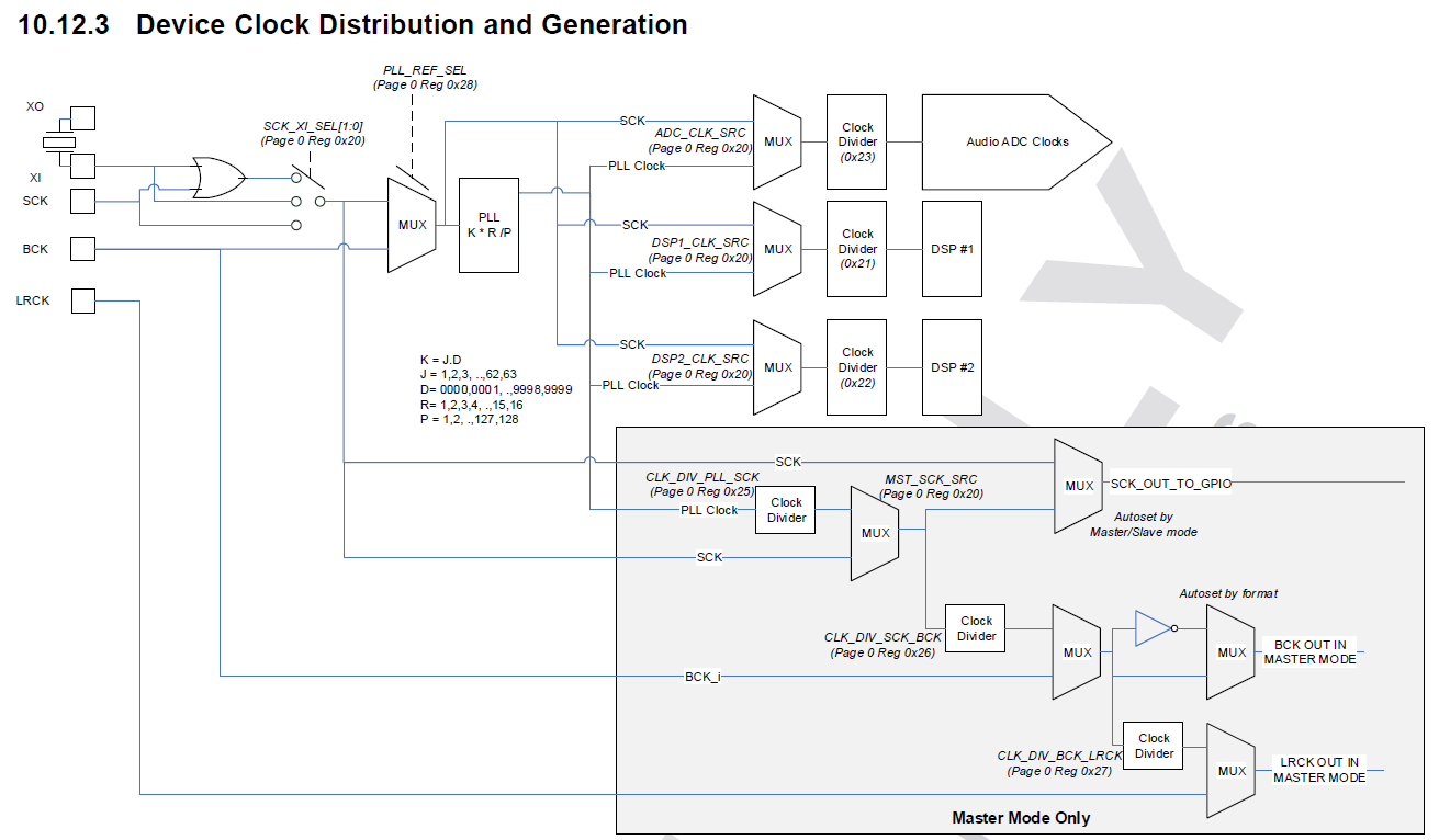
                Do we have #1,#2,#3,#4 mux register address? We can't find these register on datasheet and need them to access these mux. Thank you. 


BR

Patrick

  • Removed for NDA requirement !

  • Hi Jeffrey,

    We are working on an updated data sheet that is going through final approval now. The capture below is from the latest data sheet and has the registers for #1 and #2, however #3 and #4 are controlled by selecting Slave or Master mode:

    Red boxes: The equations should have greater than and less than symbols with the equal signs. This was a mistake fixed in the next version.

    Red box #1: This means that  the clock coming into the PLL (SCK, BCK, or XTAL) divided by the P coefficient, must be between 1 MHz and 20 MHz. For example if P = 2 and PLLCLKIN = 12.288 MHz, then 12.288 MHz / 2 = 6.144 MHz which satisfies 1 MHz <= (PLLCLKIN/P) <= 20 MHz. This case is when D of J.D is equal to 0.

    Red box #2: J is the whole number of the J.D coefficient, and must be between 1 and 63. This case is when D of J.D is equal to 0.

    Red box #3: This means that  the clock coming into the PLL (SCK, BCK, or XTAL) divided by the P coefficient, must be between 6.667 MHz and 20 MHz. For example if P = 1 and PLLCLKIN = 12.288 MHz, then 12.288 MHz / 1 = 12.288 MHz which satisfies 6.667 MHz <= (PLLCLKIN/P) <= 20 MHz. This case is when D of J.D is NOT equal to 0.

    Red box #4: J is the whole number of the J.D coefficient, and must be between 4 and 11. This case is when D of J.D is NOT equal to 0.

    Q1: Yes this should be possible, but I want to validate this with our EVM and will get back to you tomorrow.

    Q2: I calculate this by using the PLLCLK = (PLLCLKIN *R*J.D)/P, and enter in what I know and solve from there. For 48 kHz you will want a 93.304 MHz output from the PLL for the part to use. Therefore you have the PLLCLK, PLLCLKIN, and boundaries for J, R and P. From here you do trial and error to get a combination that gets you the correct output. 

    For 48 kHz:

    PLLCLKIN = 12.288 MHz

    PLLCLK = 98.304 MHz

    Try: P= 1 R = 1 J.D = 8.0

    This is also pointed out in Table 10.

    Q3: After I test my calculation on the board I will post the coefficients for 44.1 kHz.

    Justin

  • Removed for NDA requirement !

  • Hi Jeffrey,

    After doing some testing on the EVM I have the following two setups:

    For both settings:

    -auto clock config disabled (reg 0x20)

    -PLL enable (reg 0x20)

    -ADC, DAP1, and DSP clock sources are PLL (reg 0x20)

    -XTAL (reg 0x20)

    DSP1 divider: reg 0x21 = 0x03

    DSP2 divider: reg 0x22 = 0x07

    ADC divider: reg 0x23 = 0x0F

    48 kHz sampling:

    PLLCLKIN = 12.288 MHz

    PLLCLK = 98.304 MHz

    P = 2

    R = 2

    J.D = 8.0

    reg 0x2B = 0x08

    reg 0x2C = 0x00

    reg 0x2D = 0x00

    44.1 kHz sampling:

    PLLCLKIN = 12.288 MHz

    PLLCLK = 90.3168 MHz

    P = 2

    R = 2

    J.D = 7.3500

    reg 0x2B = 0x07

    reg 0x2C = 0xAC

    reg 0x2D = 0x0D

    Q4: N is the ratio of that sampling rate to the PLLCLK out. this means that if in single rate (48 kHz or below) that the ratio should be at least 2048, show in table 10 as PLL ratio. For dual rate (between 48 kHz and 96 kHz) that N should be 1024, and for quad rate (above 96 hKz) it should be 512.

    Q5: This register is to decide the ratio between your master clock and your BCK clock, this will be 64 bits *Fs. Say you have a 12.288 MHz SCK, and want a 48 kHz FS, that means you need your BCK to be 64 * 48k = 3.072 MHz. 12.288 MHz/3.072 MHz = 4. Therefore you want your MST clock to BCK (this is an error of naming, SCK should be BCK in this instance) ratio reg 0x25 should be 4.

    Q6: This will determine the PLL to SCK (or master clock), you decide what clock would work best for the master clock of the audio system that you can divide down from the PLL out clock.

    Q7: If your input clock can be evenly divided into the sampling rate, then you will not need to use the fractional part. (D not being 0).

    Justin

  • Removed for NDA requirement !

  • Hi Jeffrey,

    You are correct, you can use P = 1 and R = 1 instead, and this will meet the requirements. I was able to get the device working with both settings and will investigate with the design team as to why the limit is 6.667 Mhz and why P = 2 and R = 2 still works.

    Justin

  • Removed for NDA requirement !

  • Hi Jeffrey,

    I apologize, you are correct. We have verified with the design team and that using a crystal under 15 MHz will not guarantee that the oscillation created in the part will be stable. So far I have been testing the PLL with SCKI inputs I generated with an Audio Precision, and have ordered crystals of various frequencies to test. The EVM comes with a 24.576 MHz crystal.

    Justin
  • Hi,

    I've been trying to setup the PCM1862 for a sampling frequency of 32kHz and I am not able to see any data (with other default configs I could).

    Could you please provide the configuration to produce I2S data with the following settings to me?

     - My CLK input for SCK is 15MHz (so I tryied to manually configure the PLL, without success). I have also available a 20MHz signal.

     - I2S data word length 16bit.

     - Master mode.


    What I need is only to get the ADC data on Left and Right channels (already configured as required in reg 0x06 = 0x50) and output that via I2S with a sampling frequency of 32kHz for both signals (LRCLK  @32kHz).

    Furthermore, I think there must be also an errata on datasheet for register 0x78, reporting bad/missing status with a logic 0 instead of a logic 1... Can you confirm this? 

    Thank you very much in advance

  • Already working! I just needed to figure out the clk input (after the divider) for the ADC, which I stated it at 4.096MHz interpolating from the tables provided in the datasheet.

    I put here the most relevant register settings:

    0x20 = 0x7E;
    0x21 = 0x07;
    0x22 = 0x07;
    0x23 = 0x17; // ADC divider - 1/24
    0x25 = 0x07; // PLL divider - 1/8
    0x26 = 0x05; // SCK to BCK - 1/6
    0x27 = 0x3F; // BCK to LRCK - 1/64
    0x28 = 0x01; // enable pll
    /* PLL configuration for 98.304MHz as in the examples in the datasheet */
    0x29 = 0x00; // P = 1
    0x30 = 0x00; // R = 1
    0x31 = 0x06; // J = 6
    0x32 = 0xA0; // D = 5536d (LSBs)
    0x33 = 0x15; // D = 5536d (MSBs)

    Please review the datasheet to confirm the erratas, there is also another one in the reg32 (0x20) in MST_SCK_SRC bit saying 0: SCK or XI (default) and 1: BCK (should be PLL, right?)

    Thank you!
  • Can the public get the new datasheet? This answers some things, but this question and answer session seems messed up, perhaps something to do with the NDA?
  • Mux #2 never got identified as shown in the first post.