This thread has been locked.

If you have a related question, please click the "Ask a related question" button in the top right corner. The newly created question will be automatically linked to this question.

TAS5760M-Software mode, problem on setup the power side (no output sound)

Other Parts Discussed in Thread: TAS5760M, TAS5760XXEVM

Hi,

I am trying to make TAS5760M DAC amplifier work properly, but the are some problems I have to face and I would like community's help.

I have make my own PCB layout on a prototype version using the software mode and the I2C slave address of the TAS is routed to ground via a pull down.

While I have perfect communication with the TAS5760 through the I2C protocol(I can read and write registers), and while I have set the I2S protocol perfectly(working perfect on DS7212 codec of Dialog) I am not able to get sound through the TAS5760M that I would like to use on our production line.

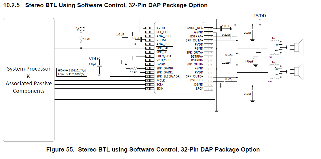
Actually the Stereo BTL Using Software Control, 32-Pin DAP Package Option Typical Application on reference manual have some misunderstood thing.


According the above steps of startup sequence  there are some misunderstood to me:

2) The !SPK_SD pin is active low, that means that the host MCU must provide the pin with logic HIGH as idle state, BUT how this could be happen as there is no power supply yet. Power supply is going to be aplied to the system on the next step(STEP 3).

4) Typical I2S host mcu protocol can only apply the SCLK and LRCK signals only if there is an ongoing playback, So how could I start 3 signals together(MCLK,SCLK,LRCK) without configured the control port first according the audio playback requirements, which is configured on the next step(STEP 5) according the steps above.

Except these I have some additional question to do:

1) There is a note that told me to bring the !SPK_SD pin LOW in order to make changes on control port via I2C, BUT that means that I have to ShutDown the playback in order to volume up for example??

2)If I am not wrong there is a reference that informs me that, toggle !SPK_SD pin is needed in order to sense the possible problem may has occur on the amplifier part of the ic, BUT according the !SPK_SD pin philosophy if I pull this pin LOW I have Shutdown state and If I pull this pin HIGH I got a non-Shutdown state, so maybe "" "Toggle" is not the right word.??

3)Is there any more spesific step by step tutorial on how to implement the Stereo BTL Using Software Control, 32-Pin DAP Package Option.

PS.:Firstly I got non-latching SPK_FAULT indication when there is no I2S data on TAS5760. After I2S data have been applied to the TAS (I mean SCLK,LRCK and DATA signals appears), i got latching  SPK_FAULT indication.

Thank you in advance 

Pelekis Marios

  • Hi, Marios,

    Welcome to E2E, Thanks for your interest in our products!.

    Please refer to my comments below:

    About your comments on the Startup sequence:

    Step 2- /SPK_SD puts the amplifier in shutdown, and is LOW active. So, in step 2 it is mentioned that the system controller should send a logic '0' (LOW) to ensure the amplifier is in shutdown during the configuration. Then, after the configuration ends, the /SPK_SD pin should receive a logic '1' (HIGH) to exit shutdown and start normal operation.

    Step 4- You can start the I²S signals before configuring the amplifier without issue. As the amplifier is in shutdown, there is no possibility of having an audible artifact caused for the digital audio format change. 

    About your additional questions:

    1. You are correct, but there is a second note after the one you mention in the typical applications section mentioning that "Any control port register changes excluding volume control changes should only occur when the device is placed into shutdown"

    2. When the amplifier detects any latching error (overcurrent, overtemperature or DC detect error), it requires the SPK_SD pin or the SPK_SD in the control port to be toggled in order to clear the error and resume normal operation. When the amplifier detects an error, it automatically shuts down the outputs to protect the IC.

    3. The steps mentioned in the datasheet are the recommended sequence to configure the amplifier.

    If you are getting a latching SPK_FAULT indication, it seems you have an OCE, OTE or DCE error.

    Best Regards,

      -Diego Meléndez López
       Audio Applications Engineer

  • Hi,Diego Melénde,

    Thank you for quick response.

    I completely understood what you told me but this is not enough to solve the problem.

    So let me tell you what I have done until now. I have make a prototype PCB following the instructions of the demo schematic on the manual at page 56.

    I leave the recommended values of the components but does not work.

    Actually I have notice 2 misunderstood on the manual:

    1) There are pins on the above print screen (Figure 55) that has as reference pin number 46,47,48 in a 32 pin chip.

    2)There are noticeable differences between the recommended schematic and the recommended layout, exist on page 69:

    Misunderstood:

    • Many of the capacitors are in differ on value(Ex. cap. on the pin 1 is 10uF against 1uF as the schematic)
    • There are extra components (Ex.Pull up resistor 10K between pin 2 and pin 32)

    Please tell me which build recommendation I have to follow and what should beware of.

    Best Regards 

    Pelekis Marios

  • Hi, Marios,

    About your comments, the schematic from the typical application section depicts the usage of the TAS5760M in SW mode with Stereo output. The IC shown in the schematic is based on the 48-pin drawing, so we need to fix the numbering, sorry for he confusion.

    The capacitor in pin 32 is used as decoupling capacitor for the voltage in the gate drive voltage regulator, and the recommended value is 1µF.

    The extra resistors you mention are related to the usage of Soft clip function in HW mode. The resistors from the layout example are used to select the voltage in SFT_CLIP pin. In SW mode, you don't need them as you can use the digital clipper instead of the soft clip feature.

    Can you please send me the register configuration so I can check it out?, also, have you tried connecting your board with out PurePath Console Motherboard to use PurePath Console 1 software and configure the amplifier?. This information will give us a better idea of what could be the issue. 

    Best Regards,

      -Diego Meléndez López
       Audio Applications Engineer

  • Hi Diego Meléndez López,

    Thank you for quick support.

    I do not have the PurePath Console so I cannot connect my board through your program.

    Except the confuse of numeration of the pins there are also differ in components value.Anyway I think it should be better work as for the manual.

    I attach my PCB's  .sch and .brb eagle's 5.6 files to see if there is something extremely fault but I am 99% sure for copy the recommended schematic from the manual.

    Also I attach the registers on the control port that asked: 

    SPK_SD(0);                                                                                                           //Hardware ShutDown

    TAS5760_Reg_WR(0x01,0xFC);                                                                      //Software ShutDown

    TAS5760_Reg_WR(0x02,0x15);                                                                       //Serial Audio Input Format is 16-24 Bits, Left Justified

    TAS5760_Reg_WR(0x06,0x71);                                                                       //Output switching rate of the Speaker Amplifier is 24 * LRCK

    TAS5760_Reg_WR(0x03,0x00);                                                                       //right channel is unmuted /left channel is unmuted                       

    TAS5760_Reg_RD(0x08,0x55);                                                                        //Read Status of register 0x08 return 0x08(A clock error is occuring)

    TAS5760_Reg_WR(0x01,0xFD);                                                                      //Software disable  ShutDown

    SPK_SD(1);                                                                                                          //Hardware disable ShutDown        

    Best Regards,

    Pelekis Marios


    Attached Eagle5.6 files:

                TAS5760.schTAS5760.brd                                      

  • Hi, Marios,

    Thanks for the additional information. Unfortunately I am not able to open the design files you provided. Can you please re-send them as PDFs or pictures?. 

    The register setting seems fine. If you are having a clock error, you may need to double check the used clock rates are compliant with the I²S Specs of the TAS5760M.

    Best Regards,

      -Diego Meléndez López
       Audio Applications Engineer

  • Hi Diego Meléndez ,

    Here I am again with Requested PDFs and the screenshot of I2S protocol communication sending to TAS5760M

    Configuation of I2S protocol:

    format.bitWidth = 16bits;
    format.channel = 0U;
    format.sampleRate_Hz = 44100Hz;
    format.masterClockHz = 128 * format.sampleRate_Hz;
    format.protocol = BusLeftJustified
    format.stereo = Stereo;

    Screenshot of Logic Analyzer. MCLK does not appear because it can not be measured from Logic Analyzer so,the  MCLK is set to 5.64MHz measured with Oscilloscope


    Attached Files:

    2086.TAS5760_BRD.pdf TAS5760_SCH.pdf

    Best Regards,

    Pelekis Marios

  • Hi, Marios,

    Thanks for the information, I have reviewed your PCB and schematic, please take a look to my comments.

    Schematic:

    • Can you please share the values of the LC filter components?, 
    • You have two inductors for each half bridge output, I guess this have debugging purposes and you use only one in your board, can you confirm?
    • Although it is not showcased in the typical application diagram, it is recommended to put a 0.1µF cap as close as possible in AVDD pin to decouple possible noises from PVDD. 

    Layout:

    • First of all, your design is done in 1-layer PCB. It is recommended to use a higher layer count PCB to provide more heat sinking capability for the TAS5760M device and to prevent traces and copper signal and power planes from breaking up the contiguous copper on the top and bottom layer.
    • The 0.1µF decoupling capacitors are located pretty far from the amplifier and after a couple jumper wires, so the decoupling effect is nullified. Not having the decoupling capacitors close to the amplifier will cause ringing on the output pins that can cause the voltage on the output pin to exceed the maximum allowable ratings, damaging the device. 
    • You may be able to improve the thermal design, by moving the components on the top and bottom of the amplifier closer to the PVDD pins, so you shall get a clear path from the IC to the cooper plane.
    • Can you please confirm if the thermal pad of the amplifier is soldered to the board?
    • +3V3 connection point is mislabeled as +15V in the layout file

    About the I²S signals, SCLK to LRCK frequency seems a little different from the 64×Fs value, but I think it is fine (32×Fs). MCLK to LRCK rate should be fine as long as MCLK frequency is 128×Fs. 

    The latching error you mentioned earlier is probably caused by the high temperature on the IC.Several factors affect the thermal performance of the IC, there is no ground layer acting as heat sink and the heat flow from the IC does not have a clear path through the edge of the board.

    Best Regards,

      -Diego Meléndez López
       Audio Applications Engineer

  • Hi Diego Meléndez,

    First of all let me tell you that what you are seeing is just a prototype PCB that has been made at the lab, that is why I am using one layer and wires.

    As for the Schematic:

    • LC Filter Values is: C=1uF, L=10uH  
    • I confirm that I use only one inductor for each output on the PCB. I put it there in the schematic, in order to have 2 inductor possible layout.
    • I put the decoupling 0.1uF capacitor as close as I could on the AVDD as you said me.Please see the newer PCB layout(attached)

    As for the Layout:

    • As I mention above I will make a better version of prototype PCB with 2 layers. I am going to make the attached layout here on lab, please confirm that it will be good.
    • Please check, on the new layout, if the distance from the 0.1uF decoupling capacitor is accepted (routed on the bottom layer)
    • I believe that it going to be more thermal effecient the new layout.
    • I can confirm that the PowerPad on the bottom of the TAS is soldered to the GND of the board.
    • I made the mislabeled 3.3V on the PCB

    Please confirm if the new layout attached on the end is it good in order to continue with the "print" of the PCB.

    The Temperature on the shell of the TAS is 40 Celsius measured with infrared thermal camera (Fluke)

    Attached Files:

    TOP_TAS5760_BRD_2.pdf  BOT_TAS5760_BRD_2.pdf


    Best Regards

    Pelekis Marios

  • Hi, Marios,

    Thanks for the information. About the schematics, I noticed that the electrolytic capacitor is connected reversed, but I think this was fixed on the board. The filter values you are providing seems fine if you are using a speaker of 4 Ohm. If using an 8 Ohm speaker, the output response won't be appropriated. You may refer to app note SLOA119b to find more information on how to select the LC filter values.

    About the PCB layout, the purpose of having two layers is to use the second layer as a heat-sink, having a big GND plane through all the bottom face, with several vias connecting top and bottom layer tom improve thermal dissipation.

    Locating the 0.1µF capacitors in the bottom layer is not recommended, you need to populate them on the same layer of the IC. The new design seems better, but I think you may be able to route a couple signals through the  bottom layer to enhance the heat flow on the top of the amplifier.

    I modified your layout in paint to make a quick example of how to enhance the thermal performance of the board. Blue is bottom layer. 

    Best Regards,

      -Diego Meléndez López
       Audio Applications Engineer

  • Hi, Diego Meléndez,

    Thank you for information, of course some things you may see in layout it is not placed in the same way on physical layout.

    Finally yesterday afternoon I order the TAS5760xxEVM, the one with ~90$ in order to test if the TAS5760  meets our requirements.

    So in a couple of days I would have make my decision. I am sorry that I giving up the effort with prototypes PCB but time is money.

    Thank you very much for continuously help,

     Pelekis Marios

  • Hi, Marios,

    Thanks for the feedback, please let me know if you need help once you receive the TAS5760xxEVM.

    Best Regards,

      -Diego Meléndez López
       Audio Applications Engineer

  • Hi Diego Meléndez,

    Yesterday I received the TAS5760xxEVM and while I connect it to my host MCU everything goes very well.

    Finally I got perfect and very clear sound from my system, via 2x8Ohm speakers!!

    So seams that some critical problem was may occurred on my prototype PCB-layout. We are going to start design the final device with TAS5760 at 32pin, opposite the once that EVM has applied(48pin), hopping that is going to work properly on a good design layout(layers-rules-heating holes-etc.).

    On the other side I would like to ask if there is any possibility TAS5760 malfunction while not in Shut Down mode and Volume is edited in parallel?

    I notice that while TAS5760 is running on the normal mode if I send to much data through I2C on Control port (Only for L/R Volume registers), there lot of times that stops the playback or stop understands the I2C incomming data.

    Is it something I could might do wrong??

    Best Regards 

    Pelekis Marios

  • Hi, Marios,

    Thanks for the feedback, I'm glad you liked the TAS5760xxEVM!. I would recommend you to take a look to TIDA-00404 design, where a TAS5760MDAP is used. You may  refer to the PCB files as a guide for designing your layout. The TAS5760M in the design is configured in PBTL mode, so you may refer to the TAS5760xxEVM for the outputs layout recommendations.

    The behavior you describe is strange, can you readback the register 0x02 to verify if there is no error reported by the amplifier?

    Best Regards,

      -Diego Meléndez López
       Audio Applications Engineer

  • Hi Marios-san,

    It seems that your schematic is incorrect since each pair of "SPK_OUTB-(23 pin) and BSTRPB-(24 pin)" and "BSTRPA-(25 pin) and SPK_OUTA-(26 pin)" is swapped in the BTL configuration.
    Please refer to the following layout and doublecheck your board.

    Best regards,
    Kato