This thread has been locked.

If you have a related question, please click the "Ask a related question" button in the top right corner. The newly created question will be automatically linked to this question.

TAS2553: Current Limit Function

Part Number: TAS2553

Dear, Sir.

I would like to confirm about Current limit function embbed in TAS2553.

i checked the datasheet, looks there are 2 kind of current limit. 

1) Class-D Output Current Limit (defined on 5 page on the datasheet). typ 3.7A. 

2) Peak Current Limit of boost (defined on 47 page on the datasheet). 2.5A. 

I am gussing ; 

TAS2553 has 2 protection function on Class-D output 1) and Boost blocks 2). 

Class-D output current limit 1) is reflected to resister 0x00 bit 1. 

I would like to get your advice my guess is correct or not. 

Best Regards,

H. Sakai

  • Hi Sakai-san,

    Sorry for the delayed response on this issue.
    You're right in your comments. TAS2553 features current limit on Class-D and it is reflected on reg 0x00 b1.
    Boost also have current limit of 2.5A as you said. One way to avoid over-current event on the boost could be to limit the battery voltage, using the battery tracking AGC. This feature is controlled with registers 0xB through 0x10 and some explanation of this function is at data sheet pages 19 and 20.

    Best regards,
    -Ivan Salazar
    Audio Applications Engineer - Low Power Audio & Actuators
  • Dear, Ivan-san. 

    Thank you so much for your advice. 

    As you mentioned, They set resister 0x02 = 0xED. It means the Battery tracking AGC is enabled. 

    Also, resister 0x0B = 0x8F (3.59V INJECTION). 

    They put 4.5V constant voltage power supply instead of the battery. 

    If resister 0x0B setting is over 4.5V, AGC will start to work depending on the output voltage. 

    It could be avoid over-current event on boost block. 

    I wonder my understanding is correct?

    Best Regards, 

    H. Sakai

  • Sakai-san,

    I think your understanding is correct.
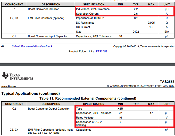
    Is the customer following the recommended values for the external components? Most specifically the inductor and capacitors near the boost pins of the device.

    Best regards,
    -Ivan Salazar
    Audio Applications Engineer - Low Power Audio & Actuators
  • Dear, Ivan-san. 

    Thank you so much for your valuable advice. 

    I would like to double-confirm. 

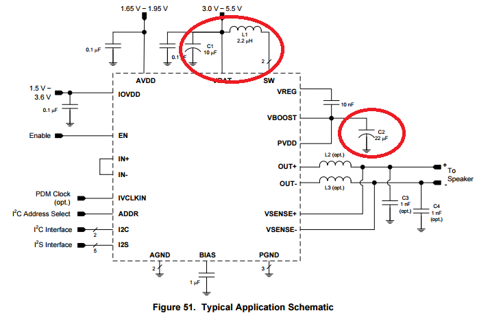
    L & C(bypass & stability) will be connected between VBAT & SW pins. 

    Do you mean these should be located near-by VBOOST pin?

    Best Regards, 

    H. Sakai

  • Sakai-san,

    I was referring to the components connected to the boost converter. I didn't want to mean that L & C should be close to VBOOST.
    I meant the recommended values for the highlighted components in the following figure:

    These should meet the recommendations from this table:

    And the text from the data sheet page 43, Boost Converter Passive Devices section.

    Best regards,
    -Ivan Salazar
    Audio Applications Engineer - Low Power Audio & Actuators