This thread has been locked.

If you have a related question, please click the "Ask a related question" button in the top right corner. The newly created question will be automatically linked to this question.

PCM2707: Still having trouble with test circuit

Part Number: PCM2707

Hello,

A while ago I attempted a very crude minimal test circuit that didn't work --- it was missing decoupling capacitors and possibly some other important connections.

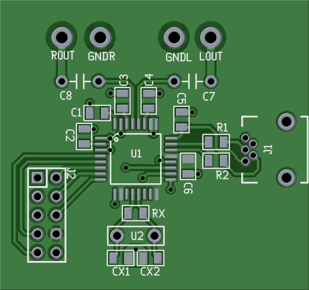
I tried this time something close to the circuit in Fig. 34 of the datasheet, except that it is bus powered (like Fig. 33).  Schematic is attached as a PNG image  (created with gEDA's gschem, then imported into PCB designer for the board layout --- a "photo-like" image export of the top view of the board is also attached --- top layer has the Vdd plane, bottom layer has the GND plane).

The thing is not recognized by the host (Ubuntu Linux --- I expect the device to appear in the Sound Settings dialog upon connecting it).  Do you see any reason why it wouldn't work?

Additional info:  bypass capacitors (C1 to C6) are: C1 = 4.7uF ceramic, 0805; C2 to C6 are 0.1uF ceramic 0805.  CX1 and CX2 are 20pF ceramic NP0, 0805  (the crystal specifies load capacitance = 12pF --- is my calculation correct?  Would 20pF be the right value for CX1 and CX2?).  RX is 1M-ohm.  R1 and R2 are 22-ohm  (all resistors are 0805).

Should I see a square wave at 12MHz at pin 13?  (I don't have an oscilloscope so I haven't tried --- I can take it to the office on Monday to check).  Please feel free to suggest any other points where I should probe and what sort of signal should I expect.

Thanks,
Carlos
--

  • Hi, Carlos,

    In general the schematic looks fine, but I have a couple comments.

    I assume that Vdd net in J2 used for monitoring only, if not, then there could be an issue as in bus powered mode, the only supply the device needs comes from the Vbus voltage on USB cable. Voltage in Vdd pin can be used to drive the digital settings of the part (like setting pin 10 to high).

    Also, it is recommended to terminate pin 15 of the device with a pullup resistor.

    About the crystal, as you mention a 12MHz signal should be seen in XTI pin. The values for CXx should be fine.

    The layout seems fine as well, but it seems weird to have the Vdd power plane in the top layer as soldering-level issues are more likely to appear with this configuration. Please make sure there is no short to Vdd plane. 

    Have you tried connecting your board to a different OS?. 

    Best Regards,

      -Diego Meléndez López
       Audio Applications Engineer

  • Thanks Diego,

    Yes, J2's Vdd pin is not connected to anything at this point, and I placed it there just in case I need to supply voltage to some low-power external device or IC.

    As for the Vdd plane --- I normally either put a power plane or just a copper-fill connected to GND.  With the PCB manufacturing company I've been using recently, I don't expect the risk to be high  (the PCB has solder masks on both sides).  Still, I will double check this detail.

    I haven't tried connecting to a different machine (different OS) --- however, there seems to be some issue with the hardware:  I don't see a 12MHz signal on either XTI or XTO.  I do see 5V at pin 24 (Vbus) and 3.3V at pin 21 (Vdd).

    Thanks,
    Carlos
    --

  • Hi, Carlos,

    Thanks for the feedback. Based on your comments, it seems that the problem could be with the crystal. The PCM2707C needs the 12MHz clock for USB and audio operations. do you have any capture of the XTx pins of the PCM device?

    Best Regards,

      -Diego Meléndez López
       Audio Applications Engineer

  • Diego Meléndez said:

    Thanks for the feedback. Based on your comments, it seems that the problem could be with the crystal. The PCM2707C  [ ··· ]


    Huh --- you specifically mention the PCM2707C;  the one I have is the PCM2707PJTR (the datasheet also mentions this code, but no mention of the 2707C anywhere).  I see that there is a separate datasheet for the 2707C;  the diagram looks the same to me, but I wonder whether there may be any important differences?

    Diego Meléndez said:

    do you have any capture of the XTx pins of the PCM device?

    Both pins show a fixed 3.3V  (well, one of them is more like 3V, the other one 3.3V).  I checked for continuity, and it doesn't look like there's any short / solder bridge between the crystal pins and the Vdd plane.

    You mentioned that the capacitors (CX1 and CX2) should be fine at 20pF.  Do you think that for sure this value is fine?  Or is it worth playing with those capacitors in case they're outside the necessary range?

    Thanks,
    Carlos
    --