This thread has been locked.

If you have a related question, please click the "Ask a related question" button in the top right corner. The newly created question will be automatically linked to this question.

TAS5630B: Device failure

Part Number: TAS5630B

Hi, 

can anybody help me?

We have a persisting problem on a borad we designed with the TAS5630B device.

First, a description of the application....

This is an audio amplifier module that fits a voice evacuation system in case of fire alarm.

The amplifier output is connected to a toroid 100V line transformer. The transformer is designed to handle 300W max, so the amplifier will provide this as a max power. Since the load connected to the transformer secondary is variable according to the number of loudspeakers installed, the amplifier will also see a variable load.

We followed all suggestions of a TI app note regarding transformer coupled amplifiers. Specifically, the transformer is designed for a 100Hz @ -3db bottom bandwidth, and the audio signal is cut at 150Hz with a 24dB/octave high-pass filter implemented on the DSP that feeds the amp. So, the transformer will never saturate.

As indicated by TI, the DSP mutes the amp until the amp is ready.

Power supply is linear, no switching, no PFC. Vdd is subject to mains fluctuations, but does never get above 52V @ 230Vac+10%

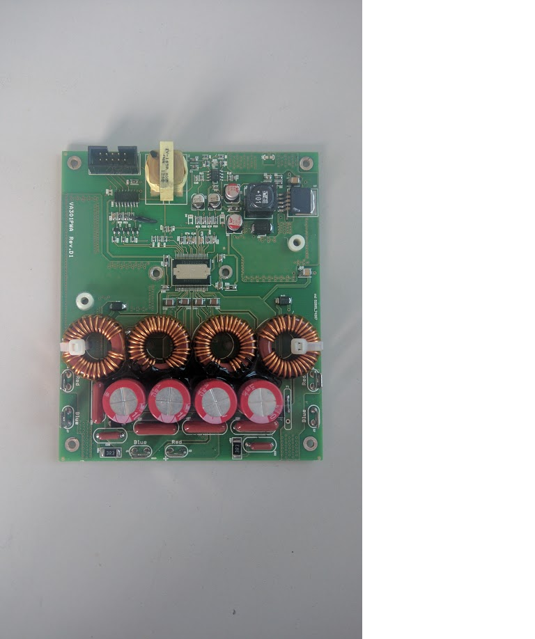
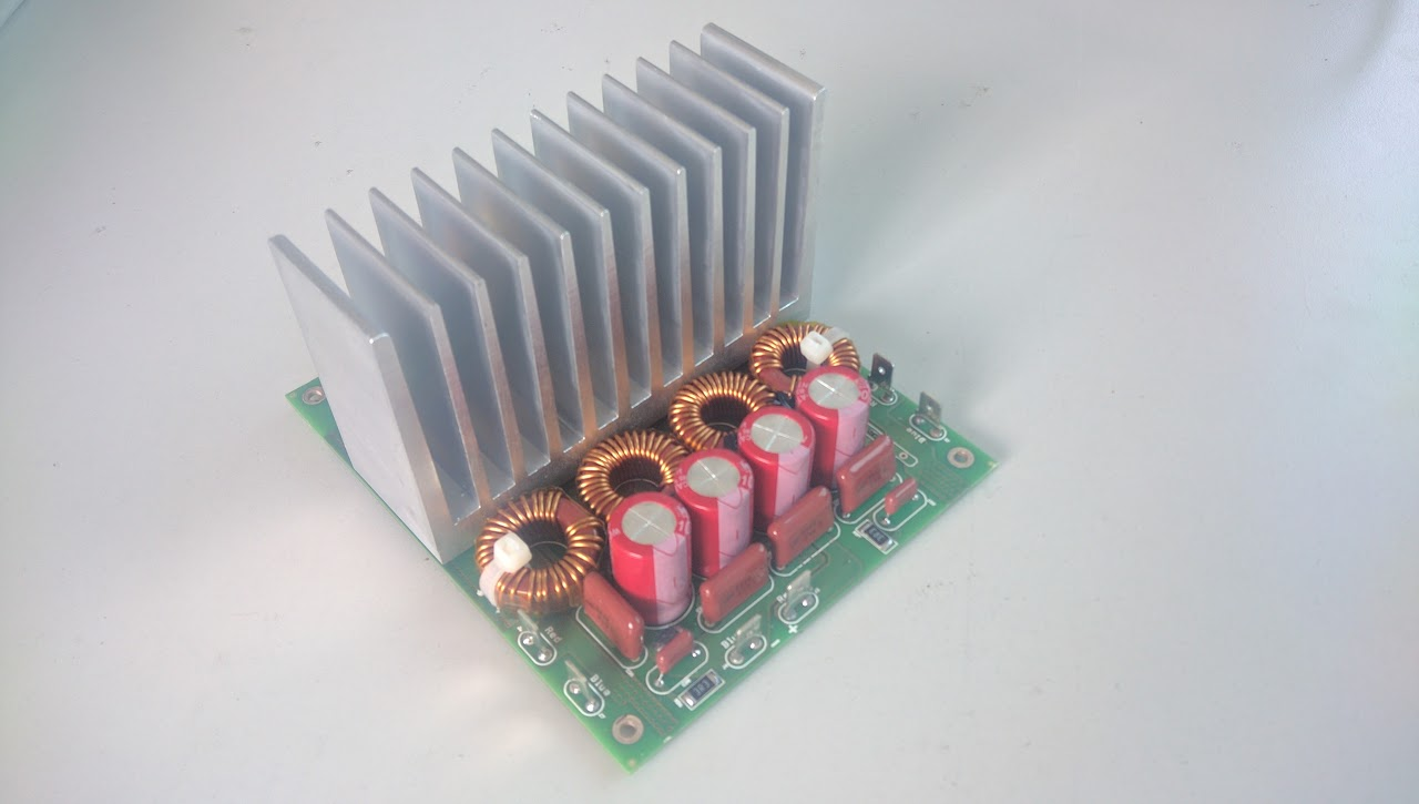
The device is PBTL configured and we designed a pcb the most similar as possible to the evaluation board. The indutors were custom made according to the specifications given  by TI for the evboard.

The input stage a copy&paste of the evboard, except for the coupling transformer since in our application, the amp needs to be isolated from the mainboard. The same goes for the status reporting pins.

On the PCB we have ground plane on the bottom side. The top side we have the 50V Vdd rail that splis into 4 legs that feed each half bridge of the device. Cose to each half bridge we have ceramic decoupling caps.

Bootstrap capacitors are on the bottom side.

The heatsink is NON-anodized alluminium to give the required strong ground connection to the heat pad. Needless to say that the holed for the screws that hold the heatsink have pads connected to the ground plane.

I have attached here both schematic and PCB layout.

I have hand mounted 15pcs prototypes with the same PCB and same compoment values. None of them failed! With these boards we have smoothly passed both EN54-16 and UL846 lab tests and product certification.

TESTING. After manufacturing, each board is tested on an automatic fixture managed by a labview application that logs the test results.

The automatic test will measure the idle current, test the reset, test the gain and perform a 2minutes  burn-in at full power (300W). The reason for the burn-in is to test the both electrical and thermal coupling of the device to the heatsink.

In order to implement similar field operating conditions, inside the test fixture the is a 100V coumpling transformer between the amp and the resistive load. The transformer is the the same that is fitted into the final application.

The same goes for the power supply: same power trasformer used for the final product.

All boards successfully pass this test. All give the same mesured data within a strict range (gain), but idle current may vary consistently from board to board: on 200 board tested, the lowest current that was measured was 140mA and the highest was 260mA @50V.

Once the amplifier board is installed in the application, the product is powered and tested from A-to-Z. The unit is loaded at its nominal and the unit is tested with a speech signal..

All units pass the functional test..

ISSUES, ISSUES, ISSUES...

Once the unit is sold  and installed by the customer, the issues arise: the amp may randomly fail after short time from power-up, or after some several weeks.

We asked to have back the broken boards to investigate the problem. All seem to be in a permanent reset state. Idle current is few milliamps (buck, opamp, etc...), nSD and READY are set low. The only way to get the board working again is to remove the TAS5630B and put a new one on it.

For our company this is a catastrophic event because all units fail once in the customer's hands!

Our new product was freshly launched and on the first 200 boards batch, 40 of them got failed!  The production manager has stopped manufacturing, sales gyus are beginning to have  a consistent backlog and the boss is knocking at my door everyday!

ANALIZING TEST LOGS AND FAULT

Each board has a SN. This helped me to do some analysis. What I have found there is a sort of correlation between the faulty boards and the idle current. All boards that failed have idle current above 200mA.

HELP HELP HELP!

Can somebody help me to investigate this issue? I really have very few options left: fixing the problem (quickly) on this board release or designing a new one, bur for sure it will not be based on a TAS6530B anymore.....

A few points here I find hard to explain:

* why on a 20pcs batch the idle current spans over a so wide range (140-260mA)? What is this due to?

* does it make sense that the boards with high idle current are more prone to fail?

* why the hand mounted units never failed, but the production ones do?

* can the failure be caused by latch-up at power-on? The primary side of the line transformer that feeds the input state is capacitor coupled to a driver ic (i.e., an opamp)

I really need all and any suggestion to address further investigation.

Many thanks for your support

Marco 

3343.VA301PWA_SCH.pdf

VA301PWA_PCB.pdf

  • Marco,

    Thanks for contacting us, let me look into this and get back to you. 

    Regards,

    -Adam

  • Thank you so much Adam!

    I desperately need some help.
    Sorry for my very long post. I tried to give you all the info I could.

    Regards,

    Marco
  • Marco,

    Just as a first thought, you mentioned the inductors were custom. Who is building them and are they closely checked?

    We care about inductance vs. current for the inductors, have you tested this? Do you have this curve you can show us?

    The main reason I think of this is because idle current is highly dominated by the output inductor. If your inductor values vary or their construction is not consistent, this could cause your idle current variation.

    A badly constructed inductor can cause an amp to become damaged depending on how severe.

    Regards,

    -Adam
  • Marco,

    Answering the other questions:

    * does it make sense that the boards with high idle current are more prone to fail?
    ~Only if the higher idle current is due to an assembly issue or an output filter issue. The higher idle current itself should not cause a failure as the device normal operation is much higher current.

    * why the hand mounted units never failed, but the production ones do?
    ~This depends on quite a few factors. It could be due to assembly differences, testing differences, etc. Can you think of any major differences in the procedure or similar?

    * can the failure be caused by latch-up at power-on? The primary side of the line transformer that feeds the input state is capacitor coupled to a driver ic (i.e., an opamp)
    ~Unsure.

    Reviewing the schematic and layout now.

    Regards,

    -Adam
  • Marco,

    The schematic looks fine to me, I don't personally have too much experience driving a transformer but others on my team do, I can ask them to take a look as well.

    I started reviewing the layout and realized that I don't see the bottom silk, can you add that please? Should be a *.SSB file.

    Regards,

    -Adam
  • Dear Adam, 

    thank you so much for your support!

    Good news that you found the schematic OK. I have no silkscreen for the bottom of the pcb. You hust have the 4 boostrap capson the bottom (C21, C25, C27, C29) These are in 0805 package and are placed just below the TAS5630B. I any case, I can send you the gerbers if you need.

    Regards,

    Marco

  • Adam,
    here some additional thoughts...

    * does it make sense that the boards with high idle current are more prone to fail?
    ~Only if the higher idle current is due to an assembly issue or an output filter issue. The higher idle current itself should not cause a failure as the device normal operation is much higher current.
    >>> Good news!

    * why the hand mounted units never failed, but the production ones do?
    ~This depends on quite a few factors. It could be due to assembly differences, testing differences, etc. Can you think of any major differences in the procedure or similar?
    >>> My prototypes and mass production are made from the same gerbers and same specifications, but the PCBs come from different suppliers.
    Maybe the inductance of the vias is different....
    The other big difference is that my prototypes are hand assembles, both SMD and PHT. Production boards are pick&place assembled and reflow soldered. My prototypes have Pb solder, production is lead-free.
    These are the mayor differences. Components are the same

    * can the failure be caused by latch-up at power-on? The primary side of the line transformer that feeds the input state is capacitor coupled to a driver ic (i.e., an opamp).
    ~Unsure.
    >>> I will decrese the value of the decoupling cap, this will shift the low pole up, but that's OK to me. Hope this helps to make the power-up transition quicker in that node.

    Regards,

    Marco
  • Adam,

    the inductors were made according to the s TIC-INDC-026(1.00) drawing from TI. I insisted with the supplier to make them with the very same T94-2 core. I have no L/I plot but since they are made upon your specifications that should be as expected. In case I may ask the supplier for that. I have tested a 20 pcs sample batch with a Fluke PM6306 RCL bridge and found that inductance is within a +/-7.4% range, that was OK to me.

    One thing I will do is to investigate again for voltage spikes on the bridge outputs and boostrap pins with a 1Ghz scope using the technique describen in your SLEA025A appnote. The purpose is to see if there is any difference between the production units and my prototypes, and of course, to check if everything is withing the absolute max ratings. I will share my findings.

    Regards,

    Marco
  • Hi Adam, 

    I have attached here the PCB gerbers, 

    hope this hepls.

    MarcoGERBER VA301PWA Rev D2.zip

  • Hi Adam, 

    how is your PCB review going. Do you have any news?

    On my side, I have investigated for spikes on the BSTx and OUTx pins of the TAS5630B.

    Please find attached here a test report.

    Unfortunately I was able to perform these tests on my lab specimen only. I need to wait for the 1st week of August to have some freshly manufactured boards with no reworks/repairs of any kind.

    I'll come back to you with the very same measurements on a mass production specimen and see if there are any differences. Maybe we'll find out that the problem is due to the PCB manufacturing and/or board assembly, but I guess it will not be so, because as you can see from the scope shots, there are no major issues. Seems like there are no overshoots to be worried about, all peaks are within abs max ratings, and ringing is well damped.

    My conclusion to such results is that there are no major parasitic things that are responsibile of these frequend failures,  and that the PCB layout is OK.

    Any comment of yours is welcome... it will make me feel relieved!

    Regards,

    MarcoVA301PWA Spike measurement report (draft).pdf

  • Marco,

    I am not done with the layout review yet, been busy :). I will get back to you today.

    Very nice test report, this looks good to me. I am interested in what we see on the production board.

    Regards,

    -Adam
  • Hi Adam,

    how are you today?

    Did some further investigations.... Friday I got back a failed board from the field. I fitted in a new TAS5630B and boostrap caps. Did the same peak measurements that were done for my hand assembled board. No significant changes.... (see attachement). By the way, this board is not as it comes from the manufacturer. It was reparied by me, but the PCB is the mass production one.

    Hope this helps...

    Regards,

    MarcoVA301PWA Spike measurement report (2).pdf

  • Marco,

    I am well, hope you are too.

    I didn't see any issues in the layout. 

    Are you able to try the test on a board that has Not been repaired by you? I understand that the boards are failing in the field but can you get one from the manufacturer and try it as the customer would receive it? My concern is that any issue that is being caused by the manufacturing is being fixed when you repair the board and obviously you cannot try it once it's already failed.

    Do you still have any failed units? If so, please measure the resistance of the bare unconnected unit in the following ways:

    1. Meaure from OUT_X to PVDD.

    2. Measure BST to OUT.

    3. Measure BST to GND.

    4. Measure PVDD to GND.

    This should help us check for damage due to output issues.

    Regards,

    -Adam

  • Hi Adam,

    No problem in taking some measurements on failed units, I should have at least one left , but others will come soon.

    I will remove the TAS5630B and make the Rdc measurements with the component off the board. Please confirm.

    Next, we have e new production batch that will be ready within a couple of weeks. I'll make the same peak measurements on them too.

    Regards,

    Marco
  • Marco,

    Please make sure you make the resistance measurements on a unit showing the same issue you reported.

    For the production batch coming out, please make sure it goes through the same testing and preparation that a customer unit would undergo.

    Regards,

    -Adam
  • Good morning Adam!

    attached here the RDC measurements I have taken on a failed TAS5630B.

    Notice that I have removed the device from the board to take the measurements.

    Because of the bias current of the multimeter flowing in one direction only, I have taken all measurement both with probes "straight" and "swapped". In the excel sheet you will find two Rdc columns.

    I will populate this file with more data as the failed boards come back from the

    field.

    Sure I will perform the very same peak voltage measurements on a borad as-it-comes from the manufacturer with all tests done and ready to be assembled in the application.

    I'll keep you posted.

    I am very curious about what you find out in the Rdc data.... I have in idea about it but I prefer keeping for myself for the moment... I'll share it with you after your feedback... I'm not willing to influence you :)

    Many thanks again!!

    Marco

    Rdc TAS5630B failed.xlsx

  • Hi Adam, 

    how are you today?

    I have a little concern about the power supply voltage....

    The datasheet states PVdd=52.5V max as the recommended operating condition and 69V as absolute max.

    What happens if PVdd is, 10% above the recommended condition (about 57.5V), but still below the abs max, including overshoots due to parasitics?

    How does this impact on the reliability of the component?

    Many thanks!

    Marco

  • Marco,

    Did this get resolved? Sorry I missed your above question.

    It is very hard to predict what might happen if the PVDD is outside of our spec unfortunately.

    Regards,

    -Adam