Dear Sir,
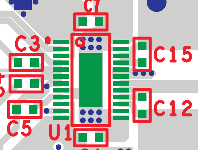
We would like to verify layout for TPA3123D2 audio amplifier. so it should not fail in EMI-EMC etc. tests. also should work well in normal operating condition.
Regards
Yogesh
Dear Sir,
We would like to verify layout for TPA3123D2 audio amplifier. so it should not fail in EMI-EMC etc. tests. also should work well in normal operating condition.
Regards
Yogesh