This thread has been locked.

If you have a related question, please click the "Ask a related question" button in the top right corner. The newly created question will be automatically linked to this question.

TPA3116D2: TPA3116 issue

Part Number: TPA3116D2

hello,for use TPA3116 I have same questions as follow,could you help give same suggestion

1. When the TPA3116 in quiescent state,the inductance is very hot,What cause this problem and how to debug it?

2. which GAIN is good for system,Generally speaking, how much is generally set

3. what is different between Gain (BTL) and Gain (SLV)

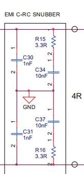
4. if output do not place below Circuit is OK,will appear bad issue?

  • Hello Darren! Shawn can help with further questions... but can you help me with some questions? What is your set-up; e.g. PVDD, load type and value,? Are you configured BTL? The gain really depends on what you are trying to do. Please reference section 7.3.1 Gain Setting and Master and Slave of the DS for guidance. The gain is typically set by your design, meaning the voltage divider that you connect to the GAIN/SLV control pin. You can also reference the EVM board for values if you are looking for a starting point. Thanks, Jeff
  • What inductors are you using? Maybe core material and/or physical construction is not suited to be used with switching devices.

    Regards,

    Christian
  • Hello Darren! Was your question answered? Thanks, Jeff
  • Hi Darren,

    Please find my answers below. 

    1. When the TPA3116 in quiescent state,the inductance is very hot,What cause this problem and how to debug it?[Shawn] This is not expected. Did you check the waveform before and affter the inductors? Does it look expected?If it is, I agree with Christian that you could check the inductor material, whether it is suited to switching application. 

    2. which GAIN is good for system,Generally speaking, how much is generally set [Shawn] The Gain setting depends on the required output power and input power. As Jeff described, you could calculate the this by output power, output load and input range. 

    3. what is different between Gain (BTL) and Gain (SLV) [Shawn] I suppose you are saying Gain(Master) and Gain(Slave). In Master mode, SYNC terminal is an output. in Slave mode, SYNC terminal is an input for a clock input. With this feature, multiple devices can be synchronized together.

    4. if output do not place below Circuit is OK,will appear bad issue?[Shawn] This circuit is used for EMI supression. The components value could be adapted for the real EMI test. But it should still work fine without this circuit, it depends on your requirement.

    Best regards,

    Shawn Zheng

  • Hi Darren,

    Does this answer your questions please? Could you please click answered if you have no other question?

    Best regagrds,

    Shawn Zheng