This thread has been locked.

If you have a related question, please click the "Ask a related question" button in the top right corner. The newly created question will be automatically linked to this question.

TLV320AIC3268: Analog input characteristic

Part Number: TLV320AIC3268

Hi All,

I am using AIC3268 in our design. Please help check:

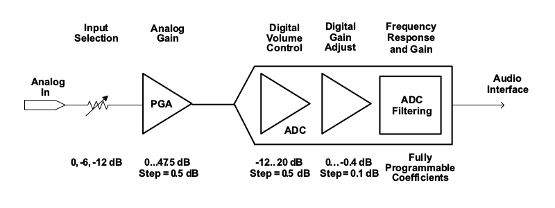
(1) ADC Single-Ended input signal level is 0.5Vrms(CM=0.9). That means it could record full-scale audio data if input level up to 0.5Vrms in single-ended mode(Rin=10K and all gain control is set to zero). The recording data will be clipped if the input level over 0.5Vrms?

(2) ADC Differential input signal level is 1Vrms(CM=0.9). It is due to the max level of each analog input(IN1~IN4) is 0.5Vrms? After differential signal merge... it will be 2*0.5Vrms = 1Vrms before enter the ADC. Is it right?

(3) 0.5Vrms or 1Vrms is a limitation for ADC analog input ? If I choose large Rin such as 40K, it could increase the max capacity of input signal level?

BR,

Steven

  • Hi, Steven,

    Please refer to my comments below:

    1- Yes, full-scale input in the digital domain is achieved with 0.5Vrms in SE mode, clipping will occur if this voltage is exceeded.

    2- Yes, the Differential input voltage spec comes from the Single-ended capabilities for each input pin.

    3- These voltages are limited by the device input capabilities, it is not recommended to provide a higher than recommended input signal.

    Best Regards,

      -Diego Meléndez López
       Audio Applications Engineer

  • Hi Diego,

    Thanks for your help!

    After aic3268 driver implemented in our custom board, I have tried to record(use alsa utility "arecord") full-scale stereo pcm data via audio interface of aic3268(AS1).:

    - The analog input signals are 1KHz sine wave on IN2L and IN1R pin.

    - The input impedances of IN2L and IN1R are 10K ohm.

    - The input common mode(CM) is 0.9V

    - All gains are zero.(I have checked analog gain, digital volume control, digital gain adjust as shown below)

    It is strange that input level must up to 1.76~1.8Vpp(about 0.63Vrms not 0.5Vrms) to achieve full-scale in the digital pcm domain.

    Are there something wrong?! or is it a tolerance?

    The analog signal on IN2L by an oscilloscope:

    The digital pcm data opened via audacity application:

    Thanks!

    BR,

    Steven

  • Hi Diego,
    I found that internal common mode CM1/CM2 selection affect recording digital level.
    In above case, CM1 is select 10K ohm such as IN2L/IN1R Rin and CM2 is not selected.

    1. Could you explain more detail about CM1/CM2? What CM1/CM2 value must be set when use single-ended mode?
    2. How about "Input Common Mode Control(B0_P1_R58)" ?

    Thank very much!
    BR,
    Steven
  • Hi, Steven,

    The purpose of having two common mode connections available is to allow effective CM resistance to be different than 10k, 20k or 40k. In Single-ended mode, the used CM should be configured to have the same input resistance value as the selected single-ended input.

    Input common mode control register is used to drive the unused inputs to the common mode voltage.  This is useful to keep the inputs at the common mode voltage for applications where the inputs are changed during normal operation.

    Best Regards,

      -Diego Meléndez López
       Audio Applications Engineer

  • Hi Diego,

    I could record full-scale data when input signal achieve 0.5Vrms now.

    Thank you very much!

    BR,

    Steven