This thread has been locked.

If you have a related question, please click the "Ask a related question" button in the top right corner. The newly created question will be automatically linked to this question.

TAS5751M: Abnormal PBTL waveform of TAS5751M

Part Number: TAS5751M


Dear All,

We got some trouble on PBTL wavform of TAS5751M.

Test conditions are PVcc=19V, RL=4ohm, Po=30W.

But there was an abnormal waveform like bellow waveform clip at about 16W output.

We think that there are some problem on PCB layout because this schematic is same as the schematic of EVM.

Also, there was no trouble on TAS5751M EVM.

Please review this PCB layout and abnormal waveform clip, then let me know the solution.

1. Schematic

2. Waveform

3. Layout

main_v01_20171012.pcb

Regards

Jeffrey

  • Hi Jffery,
    Form the scope screen, the ouput signal is not clipped, but it stops sometimes. Did you measure the waveform on the output pins? Is it continuous or not? Please also read the Error Status Register 0x02, is there any flagger error in it?
    What if outputing a lower output power? Is the output continuous? Please pay attention to the thermal performance, because the output power is high in this case.
    For the high PVDD application, please set the modulation limit(in reg 0x10) to 93.8%.
    Best regards,
    Shawn Zheng
  • Hi Shawn,

    Please refer to the bellow answers.

    Did you measure the waveform on the output pins? Yes.

    Is it continuous or not? It is continuous.

    read the Error Status Register 0x02, is there any flagger error in it?  0x02 register is read 0xC0 or 0xD0.

    Modulation limit is already set on 93.8%.

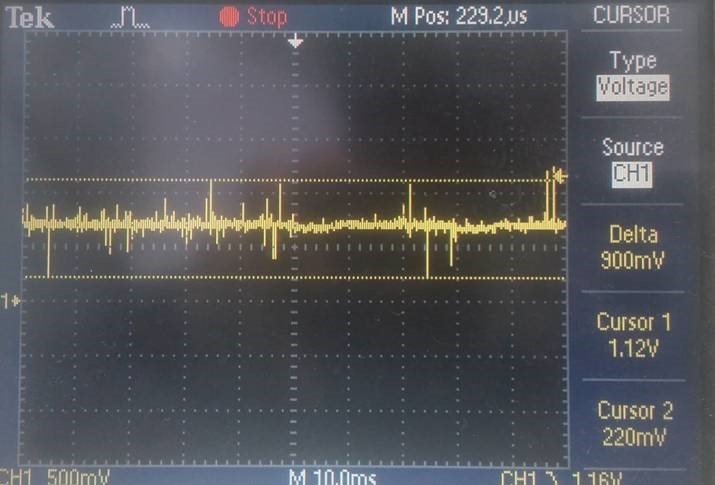
    But there are a lot of noise on PLL_FLTM pin and SSTIMER pin as bellow picture.

    1. PLL_FLTM waveform

    2. SSTIMER waveform

    Is there any idea and point for improvement of this issue?

    Please let me know that.

    Regards

    Jeffrey

  • Hi Jeffery,
    Looks like this issue is related to the I2S input. Did you check the 4 wires for the I2S input? Do they look no problem? What about the MCLK input? Please refer to the is post for the I2S clock requirement. e2e.ti.com/.../2425.i2s-clock-requirements-on-tas570x1x2x3x-device-s
    Best regards,
    Shawn Zheng
  • Hi Shawn,

    There is no problem on I2S clock. (Fs=48kHz : MCLK=12.288MHz, SCLK=3.072MHz / Fs=44.1kHz : MCLK=11.2885MHz, SCLK=2.82212MHz)
    We think that there is some problem on PLL function because noise level is so high.
    Do you have any idea or recommendation on PLL layout design guide?

    Regards
    Jeffrey
  • Hi Jeffrey,

    The I2S input clock looks good. From the above scope screen capture, the wavform looks not good. I agree with you that you could try to improve the PLL performance first. Please refer to ouor TAS5751M EVM, which is a good example for your layout design.

    Did you check the soldering on the board? Or is there any failed components on the board?


    Best regards,

    Shawn Zheng