This thread has been locked.

If you have a related question, please click the "Ask a related question" button in the top right corner. The newly created question will be automatically linked to this question.

TPA3128D2EVM: RC snubber position in the EVM Schematic

Part Number: TPA3128D2EVM
Other Parts Discussed in Thread: TPA3128D2

Hi ,

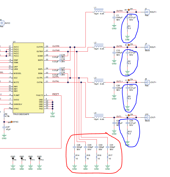
     Please clarify about the RC snubber positions in the TPA3128D2 EVM Schematic.

In this schematic , capacitor C2 connected to the  line output and Resistor R1 end connected to ground .But In the Datasheet , Resistor connected to Line output and  the capacitor  connected to ground.

So please clarify which is the correct position for these RC Snubber.

Best Regards,

Anandkumar.R

  • Hi Anandkumar,

    Sorry for the confusion. On TPA3128 EVM, we could see four snubbers on the OUT pins(in the red circle in following figure), and four snubber after the inductors on the connector(in the blue circles).

    The snubbers in the red circle is used to dampen any ringing or overshoot on the PWM output waveform to improve the performance including EMI performance. This can be reserved as option but not populated on the board. We have some materials about this. http://www.ti.com/lit/an/sloa201/sloa201.pdf  http://www.ti.com/lit/an/slva255/slva255.pdf

    The snubber in the blue circles are used to adapt the frequency response to optimize the EMI performance. The values for the capacitor and resistor in the snubber may need to be tuned/optimized according to the real EMI measurement result. Please also reserve this option for EMI tuning.

    Best regards,

    Shawn Zheng 


  • Hi,

    Thanks for your valuable suggestion.

    Best Regards,
    Anandkumar.R