This thread has been locked.
If you have a related question, please click the "Ask a related question" button in the top right corner. The newly created question will be automatically linked to this question.
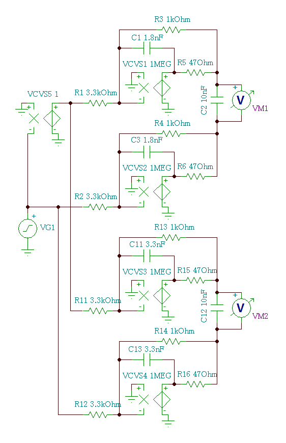
ЗСЬ1804 Manual, Figure 44 shows the schematic of the input circuit.
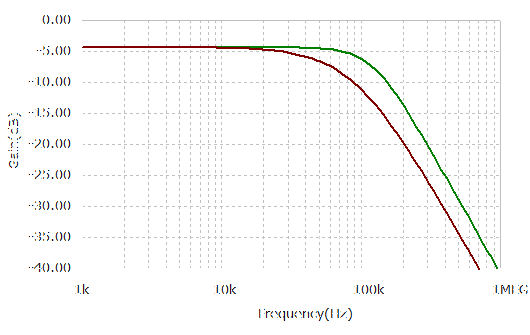
It has the 10nF capacitor at the input of the ADC, but that capacitor is compensated by using the complex feedback R3, R5 and R4, R6.
The same kind of schematic is shown on Figure 14 of OPA1632.
How does the circuit work?
How to calculate the values of the capacitor and the feedback resistors?
Hi, Dmitriy,
Welcome to E2E, Thanks for your interest in our products!.
The circuit you mention is basically an inverter low-pass filter for each differential signal, the relation between the resistors used is highlighted in the text from the APPLICATION CIRCUIT FOR SINGLE-ENDED INPUT section on the document.
Best Regards,
-Diego Meléndez López
Audio Applications Engineer
Hi, Dmitriy,
I think the circuit you mention is similar but it is not the use case for the PCM1804. The purpose of the input circuit from Fig. 44 is to provide a differential input to the PCM1804 from a single-ended source. The first op-amp in the signal chain is an inverter with unity gain. The 10µF cap on each line is used to remove the DC offset from the single-ended input source, then a low-pass filter is implemented on both legs to remove the out-of band noise of the input source and atttenuate the signal to make it compatible with the input specs for the PCM1804.
Best Regards,
-Diego Meléndez López
Audio Applications Engineer
Hi Diego,
I think there is some misunderstanding.
See PCM1804.pdf, Figure 44. The lowpass filter is R1-C(1) and R4-C(1).
See OPA1632.pdf, Figure 14. The lowpass filter is R3-C1 and R4-C2,
But what do the 0.01 uF capacitor, Figure 44, PCM1804.pdf? What do C3 2.7nF, Figure 14, OPA1632.pdf?
Why the schematics use that capacitor if it is compensated by the loop back?
Best regards,
Dmitriy
Hi, Dmitriy,
The 0.01µF capacitor from the PCM1804 datashee along with R6 and R5 forms an antialiasing filter for the ADC input. Same situation with C3, R5 and R6 from the OpAmp Datasheet.
Best Regards,
-Diego Meléndez López
Audio Applications Engineer
Hi, Dmitriy-san,
I have analyzed this LPF circuit few years ago. This circuit constitutes a 2nd order LPF. The transfer function is as follows.
H(s)=-R3/(R1*(R3*R5*C1*C2*s^2+(R3+R5)*C1*s+1))
where C1=C(1)=1800pF or 3300pF, C2=2*0.01uF
ωc=1/√(R3*R5*C1*C2)
Q=(R3+R5)/√(R3*R5*C2/C1)
when R3=1kΩ, R5=47Ω, C1=0.0018uF, C2=0.02uF
Fc=ωc/2π=122.35kHz, Q=0.69
when R3=1kΩ, R5=47Ω, C1=0.0033uF, C2=0.02uF
Fc=ωc/2π=90.365kHz, Q=0.51
I show TINA-TI simulation of this LPF below.
Akio Ito
Hi, Akio-san,
Thank you for your explanation!
You are right, this is the 2nd order lowpass filter.
Now I understand how to calculate it.
Best regards,
Dmitriy