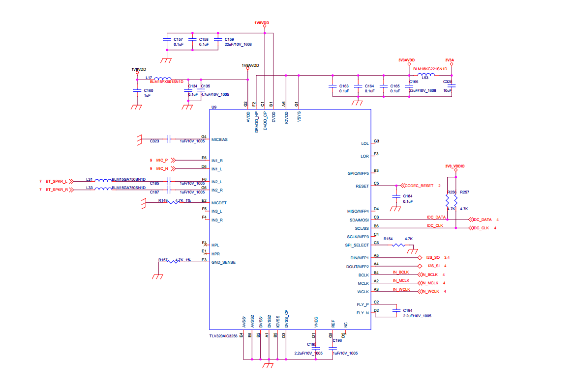
Part Number: TLV320AIC3256
Channel 1 is MIC input. SE in. external MIC bias.
Channel 2 is BT speaker. Diff. in.
below is my register table, please help me check any wrong?
when i only channel 1 or only channel 2 input, there is no any noise.
but when i both Ch1 & Ch2 input, there is noise issue here.
static const RegValue RecordingBothOn[] = {
	//{0x00, 0x01},	//# switch to page1
	//{0x33, 0x40},	//# Enable MICBIAS and set to 1.25V, MICBIAS voltage is generated from AVDD
	{0x00, 0x00},
	{0x3D, 0x01},
	{0x00, 0x01},
	{0x01, 0x08},
	{0x02, 0x00},
	{0x3D, 0x00},
	{0x47, 0x32},
	{0x7B, 0x01},
	{0x00, 0x01},
	{0x33, 0x00}, //40

#ifdef CONFIG_TARGET_BOARD_R1_PRO
//	{0x34, 0x33},	//# IN1R, IN2L						is routed to Left MICPGA POSITIVE with 40K resistance
//	{0x36, 0xF0},	//# 	  IN2R		 	CM1L, 		is routed to Left MICPGA NEGATIVE with 40K resistance
//	{0x37, 0xF0},	//# IN1R, IN2R						is routed to Right MICPGA POSITIVE with 40K resistance
//	{0x39, 0xCC},	//# 	  	,			CM1L		is routed to Right MICPGA NEGATIVE with 40K resistance

	//{0x34, 0x22},	//# IN1R, IN2L						is routed to Left MICPGA POSITIVE with 40K resistance
	//{0x36, 0xA2},	//# 	  IN2R		 	CM1L, 		is routed to Left MICPGA NEGATIVE with 40K resistance
	//{0x37, 0xA2},	//# IN1R, IN2R						is routed to Right MICPGA POSITIVE with 40K resistance
	//{0x39, 0x82},	//# 	  	,			CM1L		is routed to Right MICPGA NEGATIVE with 40K resistance

	//{0x34, 0x02},	//# only mic /20K
	//{0x36, 0x82},	//#
	//{0x37, 0x80},	//#
	//{0x39, 0x82},	//#

	//{0x34, 0x20},	//# only BT /20K
       //{0x36, 0x20},	//#
	//{0x37, 0x22},	//#
	//{0x39, 0x00},	//#


	{0x34, 0xf3},  //0x55  //0x8a
	{0x36, 0xf3},
	{0x37, 0xf3},   //0x44 //0x88
	{0x39, 0xf3},
#endif
#ifdef CONFIG_TARGET_BOARD_10C_EVO
#if 0  // 20K
	{0x34, 0x0A},	//# IN1R,		IN3L				is routed to Left MICPGA POSITIVE with 40K resistance
	{0x36, 0x8A},	//# 			IN3R,	CM1L,		is routed to Left MICPGA NEGATIVE with 40K resistance
	{0x37, 0x88},	//# IN1R,		IN3R				is routed to Right MICPGA POSITIVE with 40K resistance
	{0x39, 0x8A},	//# 			IN3L,	CM1L		is routed to Right MICPGA NEGATIVE with 40K resistance
#else  // 40K
	{0x34, 0x0F},	//# IN1R,		IN3L					is routed to Left MICPGA POSITIVE with 40K resistance
	{0x36, 0xCF},	//# 			IN3R,	CM1L,	CM2L	is routed to Left MICPGA NEGATIVE with 40K resistance
	{0x37, 0xCC},	//# IN1R,		IN3R					is routed to Right MICPGA POSITIVE with 40K resistance
	{0x39, 0xCF},	//# 			IN3L,	CM1L,	CM2L	is routed to Right MICPGA NEGATIVE with 40K resistance
#endif
#endif

	{0x3B, 0x28},	//# Left MICPGA Gain is enabled, Left MICPGA Gain is set to 0dB 08
	{0x3C, 0x28},	//# Right MICPGA Gain is enabled, Right MICPGA Gain is set to 0dB 08

	{0x00, 0x00},	//# Select Page 0
	{0x53, 0x00},	//# Left ADC Channel Volume = 10dB 14
	{0x54, 0x00},	//# Left ADC Channel Volume = 10dB 14
	{0x51, 0xC0},	//# Power up LADC, Power up RADC
	{0x52, 0x00},	//# Unmute LADC, Unmute RADC
};