This thread has been locked.

If you have a related question, please click the "Ask a related question" button in the top right corner. The newly created question will be automatically linked to this question.

TPA3251D2EVM: TPA3251D2

Part Number: TPA3251D2EVM

We have designed a driver amp for a special purpose that is similar to a sub-woofer amp function.  DC to 250hz response.    The TPA3251D2 looked better than our previous attempt so we have designed around it.  The one problem the customer dislikes, is the shut down when hitting full power plus output.  Rather than just clipping like a normal amp, as soon as the output gets to >101% the OI protection is tri-stating the outputs for a short period of time, thus causing tremendous distortion in the load even with just 8 ohms.   I have verified all reference supplies are stable with a scope.  This appears to be the internal protection causing this.  Reading another post on PFFB design, I was wondering if this might to some degree lessen this effect.  I am being forced to design and add a brick wall limiter if not.  Even with light loads this shut down of the outputs appear.  What can be done?  see  https://www.dropbox.com/s/eu92she69zm8iig/200w%20Amp%201.pdf?dl=0

  • Darrell,

    Could you clarify the PVDD, output voltage, and load you are using when you see the issue?

    Regards,

    -Adam

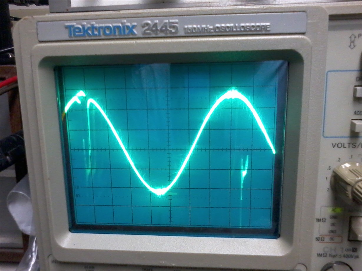
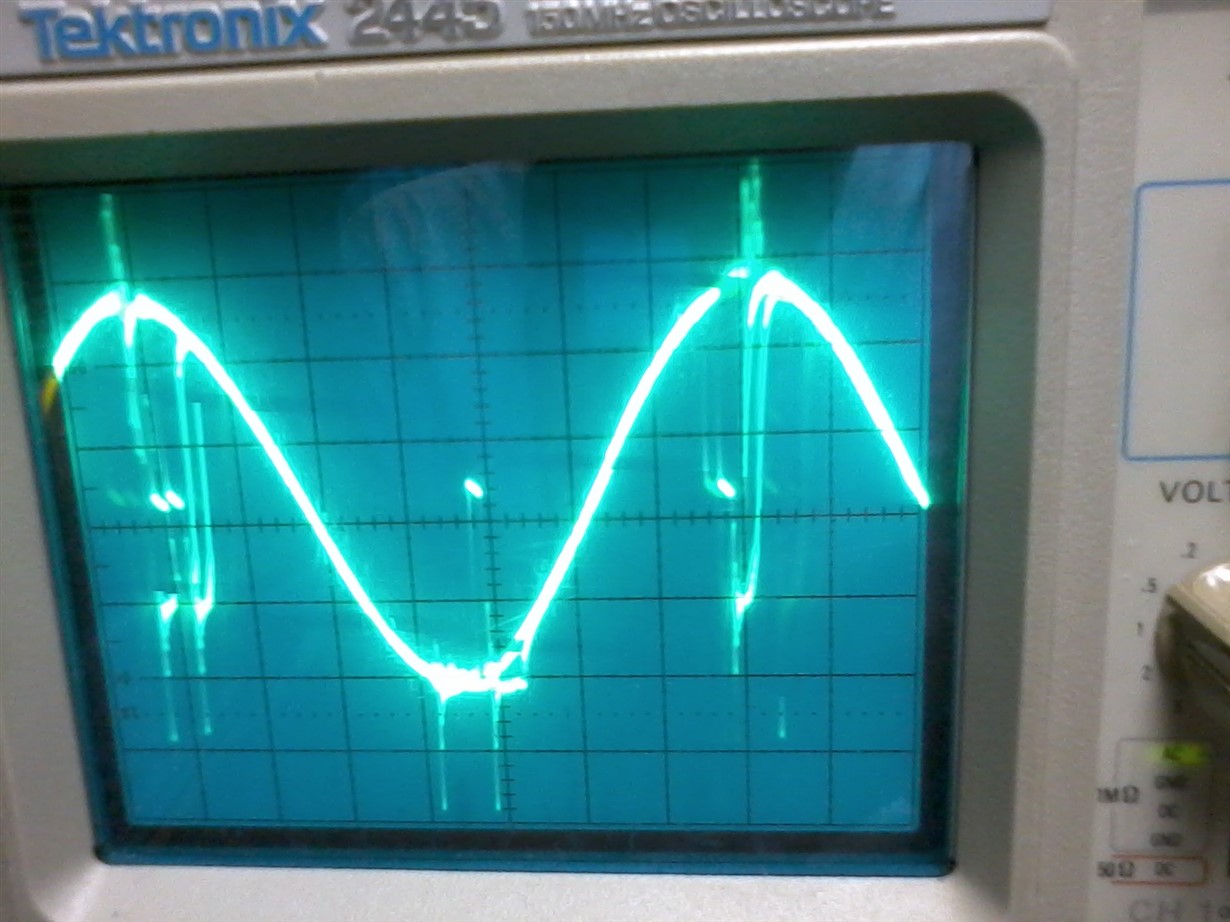
  • Thank you for a reply.  Attached are two pic's of the clipping first with no load and second with 7ohm dummy load (non-reactive).  If this is due to the PWM's overlapping and causing a common mode current, why would TI design an amp like this, seems to be to be a simple task to add circuitry such that overlap of the two PWM signals never can happen internally . The amp should then clip like a normal AB amp at the rail and there would be no common mode current.  This is the type of functionality I need.  PS the part is in dual BTL mode.  config bits, 00.  If there anything I can do to change this in my design?

    I have check and verified there is no RF on any of the power pins of the device.

    PVDD is at 30Vdc

      Thanks

    7 ohm load

  • FYI our previous successful design was with the TAS5121 part. It did not have this type of shut down / clipping. Sorry, it reminds me of the inversion problem with non rail to rail op-amps.
  • Darrell,

    I can assure you that our amp never allows the PWM edges to overlap, this is a vital spec of ours and it cannot be violated. I tried this on our EVM in both no load and 8R load and I didn't see the same behavior. Is this happening on your board? Have you tried a different board or the EVM?

    What is the frequency of the sine shown?

    Regards,

    -Adam
  • Sign wave is 100hz. We have built 50 of these as prototypes, I believe others do it, but I will have to check.

    This is with our board and not with an Eval unit. I sent you a link to the schematic, did you get it. It is basically a copy of your reference designs in the spec sheet. Glad to here about the non-overlap of the PWM in your design. SO with no load what is happening?

    There should be little to any current with no load, unless you think the filter inductor is saturating and the filter currents are high. we used a 10uh 11A inductor and high quality 200v MLCC caps in the output filter.
    The inputs are driven in differential mode and have about 4Vp-p when the amp starts clipping. Could we be clipping the input?

    Output power is right at expected power level for max output under load just before the break up. One difference is the eval board has 100ohm resistors in series with the input pins. Could this be a layout problem even with no load? Pvdd caps are not as close as in your design.
    When the problem happens only the clip output is going true.
    AVDD is at 7.75v no signs of noise
    DVDD is at 3.3v no signs of noise
    PVDD is at 29v no signs of noise but there is a little droop
  • MORE INFO:

    I have modified my R-R op-amp driver stage such that I can change the maximum output via the VCC on the part, in this way limiting the max p-p output V.  After doing this the power amp stage no longer does , what looks like phase inversion when achieving max power output.

       I can even overdrive the amp and get up to 200w out of a 140w much like a normal AB would act, due to the clipped sign wave duty cycle effect.  This tells me it is NOT current limiting at all but the input must be inverting like an old op-amp design.

      There is very little information in any document about the inputs on this device.  The EVAL board has 12v rails on the driver amp, I am surprised you can not duplicate this.  Unless this is a one off failure with this part. I will have to check for this on other units. 

  • Darrell,

    The 100ohm on the input is for the 16MHz low-pass filter.

    So it sounds like the issue is resolved, we are just trying to understand the phenomenon?

    I just drove 12V p-to-p deferentially at 100Hz pre-op-amp into 8ohms on the output, and while the amp reached ~30% THD, I saw no phase inversion as you mention. I'm suspecting an issue with your op-amps, can you scope the input?

    Regards,

    -Adam

  • I did scope the inputs along with everything else, the inputs are perfectly clean. This is a simple change to our design and we will use this for now. However, like you I would really like to know why. It does not seem to be current in the load related. Maybe it is a one off bad part or this production run, I will have to test other units to see if this is true. Most are already at a beta site customer. Can we leave this thread open for now until I get more info, or can I contact you directly? Ether way I wonder what the designer/production test people think about this. Regards Darrell
  • Darrell,

    We will need to close this thread for now if the issue is resolved but you can ask a related question here by clicking the "Related Question" button or email me directly at adamsidelsky(at)ti(dot)com.

    Regards,

    -Adam


    If your question was answered, please click the "This resolved my issue" button!