This thread has been locked.

If you have a related question, please click the "Ask a related question" button in the top right corner. The newly created question will be automatically linked to this question.

Linux/TLV320AIC3104: TLV320AIC3104 mic input config failed

Part Number: TLV320AIC3104


Tool/software: Linux

【Chip model】:
TLV320AIC3104
【Platform】:
Qualcomm MDM9607
【Problem Description】:
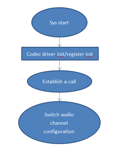
Initial plan:
Mic1 left channel input, Right_LOP/M output
There is no problem with this solution.

Current modified plan:
Two channels are used, which are the left mic1 input to the Right_LOP/M output, and the other is the mic1 right input to the LEFT_LOP/M output.
Two channels need to switch between two channels according to demand.

The following four lines, in theory, can control the direction of a single input, but the configuration will not fully take effect afterwards.


Input1 has two input directions, line 1 is connected to Left-ADC and line 4 is connected to Right-ADC.
Input2 has two input directions, line 2 is connected to Right-ADC and line 3 is connected to Left-ADC.
According to our needs, one path is input1 line 4 is connected to the Right-ADC, and the input2 input path is completely disconnected.
The other path is input2 line 3 is connected to the Left-ADC, and the input1 input path is completely disconnected.
The problem arises here. When the input1 line 4 is connected to the Right-ADC and all the input2 input channels are disconnected, the input2 operation register configuration is not valid, and the sounds input by input1 and input2 are simultaneously broadcasted from the output channel; When using input2 line 3 to receive Left-ADC, all disconnect input2 input path, disconnect input2 operation register configuration does not take effect, input1 and input2 input sounds are simultaneously broadcast from the output channel;
The following is our register configuration:

Init configuration:

Input1 channel selection configuration:TLV320AIC3104-Q1_issue.docx

Input2 channel selection configuration

Please help to check if there is a problem with the configuration of the villager. Why does it fail to close lnput?

  • User,

    I'm not sure I am clear on what your problem is, can you post some diagrams showing what you want to do? perhaps your register configuration?

    best regards,
    -Steve wilson
  • dear sir
    Please see the attached document with a screenshot showing my solution configuration problem.TLV320AIC3104-Q1_issue.docx

    thanks
  • dear sir

    Please see the attached document with a screenshot showing my solution configuration problem.

    As shown in the second image above, we need to configure #1 #2 #3 #4 four paths, #1#4 #2 path disconnect, #3 path open, or #1 #4 #2 path disconnect, #3 Path open, #4 open, #1#2#3 path closed
    According to the chip manual, the following registers should be configured separately. R19 R21 R22 R24
    The following is our register configuration, two mic will still work at the same time

  • #1#4 #2 Path disconnected, #3 lane connected, or #1 #2 #3 pathway disconnected, #4 pathway connected
  • dear   sir

    Have you understood our current problems?

    any update ?

    thanks

  • User,

    I noticed two things.
    First: When you are using the input to drive the PGA you configure it as a differential input, but when you disconnect that input from the PGA, you configure it as a Single Ended input. if it is a differential input always configure it as a differential input.

    Second: your second register configuration shows register 24 with a value of 0x7C. this should be 0x78 as the 3 least significant bits are all reserved.
    please make those changes and test.

    best regards,
    -Steve Wilson
  • dear sir
    The following is the register configuration I used mic1 left to call, found that mic1 right still has voice input
    [ 798.869831] writer register 0x0 vulae 0x0
    [ 798.874204] writer register 0x13 vulae 0xfc
    [ 798.878088] writer register 0x15 vulae 0xf8
    [ 798.881926] writer register 0x16 vulae 0xfc
    [ 798.886889] writer register 0x18 vulae 0x80
    [ 798.891385] writer register 0x52 vulae 0x80
    [ 798.895312] writer register 0x5c vulae 0x80
    [ 798.900329] writer register 0x29 vulae 0x50
    [ 798.904384] writer register 0x2b vulae 0x80
    [ 798.908057] writer register 0x2c vulae 0x0
    [ 799.220030] writer register 0x56 vulae 0x6b
    [ 799.225303] writer register 0x5d vulae 0x6b
    [ 799.229610] writer register 0xf vulae 0x28
    [ 799.233014] writer register 0x10 vulae 0x28
  • dear sir:
    When I configured R19 as 0xf8, there was no sound input from both mics.
    When I turn the Right-ADC off, both mics still have sound input.
    Therefore, the configuration of the Right-ADC is invalid, the Left-ADC can be configured, but the input of the mic cannot be completely turned off.
    Does this ic have configuration problems with this scenario in other users?

    thanks
  • User,

    The TLV320AIC3104 has been released since 2008 or so, the AIC33 which is the platform upon which the AIC3104 was based was released even earlier, 2006 or so. In the time it has been released there is no documented instance of this problem. are you using an EVM? is it brand new or has it been used before? if it has been used before, was it used for any ESD testing? or were the ABSMAX rating exceeded?

    I just tested your configuration on my EVM and I do not have a problem. As expected ,when LINE1R is connected to the left ADC i only hear LINE1R, when line1L is connected to the right ADC I only hear LINE1L.

    what is your input level? you will need to provide more details regarding your testing.

    best regards,
    -Steve Wilson
  • dear  sir:

    This ic is brand new, has not been used before, and has not done aging test. Is there any problem with my configuration? Is the input level saying gain or voltage?

    Your demo board test is normal, it is reasonable to say that it should support this functional requirement.

    Now I really have this problem on my side? How to investigate next?


    I will provide a codec schematic to help check the circuit.


    All initialization configurations and channel switching configurations are documented


    Also need what information we provide, please describe a specific point

  • dear sir
    The input voltage of mic1L is 8V
    mic1R has no input pull-up

    Please note.
    thanks
  • dear sir
    mic1R has no input pull-up
    The input pull-up of mic1L is 8V

    thanks
  • dear sir:
    any update?

    thanks
  • User,

    Provide detailed description of your test setup. Explain everything in detail. How connections are made, how measurements are made, every single register write you make to the AIC3104. If possible show us your test setup.

    I have tested what you think your configuration is, and it works just fine for me. One thing to try is read the registers 19-24 to confirm that they match your configuration

    best regards,
    -Steve Wilson
  • User,

    wait... the mic input swing is 8V?  You of course realize that the ABSMAX for the input pins is AVSS-0.3V to AVDD+0.3V right?

    if AVDD =3.3V  then this input range is  -0.3 to 3.6V.    If you lower the input voltage to within the proper input levels and the behavior is still incorrect,  it is likely that you damaged the device.

    Best regards,

    -Steve Wilson

  • dear sir

    Please check the schematic I sent, although our input voltage is 8V, but there is a peripheral protection circuit. 8V is the MIC DC power supply, and there is a DC blocking capacitor between the codec. The actual input signal amplitude is about 1V. Please help check if there is a problem.
    I have read the registers R19~R24, which is indeed the value I wrote.
    And adc mute is the normal operation.

    thanks

  • dearsir

    My steps are as follows:

    1.When the system boot driver is initialized, configure it as document TLV320AIC3104-Q1_issue.docx Init configuration:
    2.After the system starts, when you start making a call, first switch the channel and perform register configuration such as Input1 channel selection configuration:
    Another channel switch register configuration is called Input2 channel selection configuration.

    thanks

  • dear   sir:

    The specific two data channels are as shown in the figure below. The green arrow part represents one channel input1, the corresponding output channel is output1; the red arrow represents one data channel input2, and the corresponding output channel is output2;

  • User,

    Again, I have setup the AIC3104 using your configuration and it works just fine.

    1. can you run your "input1 channel selection configuration" and then read registers 15-24?
    2. then run your "input2 channel selection configuration" and read the registers 15-24 again.

    best regards,
    -Steve wilson
  • dear sir
    I've read the values of the R19 to R24 registers, which are the same as the values I wrote.
    Is there any problem with our schematic circuit design?
  • User,

    C902 is not populated, correct? There should be no capacitor there.

    regarding the IN1R input, Is this microphone single-ended? if so, the negative terminal of this mic should go directly to gnd, and C910 on the IN1RM pin should go to GND.

    best regards,
    -Steve Wilson
  • dear  sir:

    Capacitor C902 does not have a sticker,We didn't use micbias.

    mic1R is differential input mode,

    the negative terminal of this mic:

  • User,

    Ok, I would recommend not calling that node "MIC_IN_GND" as it isn't a GND.

    We are at a point where I have seen your configuration and schematic and both look good. I've tested your configuration on the EVM and it works fine. There is also no past history with the TLV320AIC3104 and this problem (the test program would weed any chips that failed this test anyway)

    Have you also tested multiple AIC3104 devices? any chance this device could have been damaged?

    I would like to see your test setup. A picture or a block diagram showing your test setup, and measurements of input and output signals.
    Please show as many details as possible.

    -Steve Wilson
  • dear  sir
    mic1R and mic1L are all working in differential input 

    We have replaced four devices to do the test, all have the same problem.

    Here is my test step

    Driver initialization register configuration
    And the detailed configuration of the register for channel switching has been described in the previous reply.

    measurements of input and output signals would be provided later

    What is currently suspected?

  • User,

    Please provide an entire register dump for this device. Read every single register on page 0 and provide the full readout here.

    also, if you could provide the details I asked for about your test setup, that would still be helpful. I want to know EXACTLY how you are testing this. I've mentioned many times that I have tested your configuration and it works fine on my end. knowing the history of AIC3104 failures, and that you have also tested 4 different devices leads me to believe that this is not an issue with a damaged/faulty device. So something is amiss. Either your test procedure is faulty, or the configuration you've provided me with is not complete.

    Also, please provide a screenshot of the I2S lines. the BCLK, Wclk, DIN, and DOUT.

    best regards,
    -STeve Wilson
  • dear  sir:

    I don't quite understand what you need "about your test setup," specifically, what are the steps, I have already drawn a block diagram for you.

    The following is all codec related operation flow register configuration and register dump;

    The BCLK, Wclk, DIN and DOUT waveforms of the I2S series are provided later.

    initial codec registers:
    1)pull the reset gpio to reset 
    2)write registers:
    The following are all register initialization configurations. Other unconfigured registers are set by default.
     {0x00,0x00},//select page 0
        {0x2a,0x9c},//page 0 Register42 Driver Power-on time 800ms,Rame-up 4ms
        {0x13,0xfc},//R19//IN1LP/IN1LM differential mode and Left-ADC control-It should be differential mode not single-ended mode,otherswise it will create a DC-offset
     {0x15,0x80},//R21//IN1RP/IN1RM differential mode and Left-ADC control
     {0x16,0xfc},//R22//IN1RP/IN1RM differential mode and Right-ADC control
     {0x18,0xf8},//R24//IN1LP/IN1LM differential mode and Right-ADC control
     {0x0f,0x00},//Register 15 Left-ADC PGA Gain
     {0x10,0x00},//Register 16 Right-ADC PGA Gain
     {0x07,0x0a},//data path Left_DAC->left input Right_DAC->Right input
     {0x25,0xc0},//Register 37 L/R_DAC power
     {0x2b,0x00},//Page 0 Register 43 Left-DAC Digital Volume Control
     {0x2c,0x80},//Page 0 Register 44 Right-DAC Digital Volume Control
     //{0x51,0x80},//PGA_L to Left_LOP/M
     {0x52,0x80},//DAC_L1 to Left_LOP/M Register 82
     //{0x54,0x80},//PGA_R to Left_LOP/M
     //{0x55,0x80},//DAC_R1 to Left_LOP/M
     //{0x56,0x80},//Page 0 Register 86 Left_LOP/M Volume Controla
     //{0x58,0x80},//PGA_L to Right_LOP/M
     //{0x59,0x80},//DAC_L1 to Right_LOP/M
     //{0x5B,0x80},//PGA_R to Right_LOP/M Page 0 Register 91
     {0x5c,0x80},//DAC_R1 to Right_LOP/M Page 0 Register 92 Volume Control
     //{0x5d,0x80},//Page 0 Register 93 Right_LOP/M Volume Control
     {0x29,0x50},
     
    config 3104 Registers for switch to channel1 :
    [ 2458.619054] writer register 0x0 vulae 0x0
    [ 2458.622505] writer register 0x13 vulae 0xfc
    [ 2458.627621] writer register 0x15 vulae 0xf8
    [ 2458.632379] writer register 0x16 vulae 0xfc
    [ 2458.637814] writer register 0x18 vulae 0x80
    [ 2458.641359] writer register 0x52 vulae 0x80
    [ 2458.646045] writer register 0x5c vulae 0x80
    [ 2458.650690] writer register 0x29 vulae 0x50
    [ 2458.654394] writer register 0x2b vulae 0x80
    [ 2458.658821] writer register 0x2c vulae 0x0

    adjust volume
    #unmute when voice start
     echo 0x56 1 0x6b > ${reg_val}
     echo 0x5d 1 0x6b > ${reg_val}
     #mic 20dB
     echo 0x0f 1 0x28 > ${reg_val}
     echo 0x10 1 0x28 > ${reg_val}

    end voice
      #mute before end voice
     echo 0x56 1 0x02 > ${reg_val} 
     echo 0x5d 1 0x02 > ${reg_val}
    dump 3104 Registers:
    [ 2458.673517] ti3104_i2c_read_byte:reg[0x0] = 0x0,ret = 2
    [ 2458.678321] read register 0x0 value 0x0
    [ 2458.990787] ti3104_i2c_read_byte:reg[0x1] = 0x0,ret = 2
    [ 2458.996204] read register 0x1 value 0x0
    [ 2459.309479] ti3104_i2c_read_byte:reg[0x2] = 0x0,ret = 2
    [ 2459.314431] read register 0x2 value 0x0
    [ 2459.630537] ti3104_i2c_read_byte:reg[0x3] = 0x10,ret = 2
    [ 2459.636404] read register 0x3 value 0x10
    [ 2459.950063] ti3104_i2c_read_byte:reg[0x4] = 0x4,ret = 2
    [ 2459.957723] read register 0x4 value 0x4
    [ 2460.270873] ti3104_i2c_read_byte:reg[0x5] = 0x0,ret = 2
    [ 2460.276337] read register 0x5 value 0x0
    [ 2460.592579] ti3104_i2c_read_byte:reg[0x6] = 0x0,ret = 2
    [ 2460.597582] read register 0x6 value 0x0
    [ 2460.909216] ti3104_i2c_read_byte:reg[0x7] = 0xa,ret = 2
    [ 2460.915380] read register 0x7 value 0xa
    [ 2461.227896] ti3104_i2c_read_byte:reg[0x8] = 0x0,ret = 2
    [ 2461.233386] read register 0x8 value 0x0
    [ 2461.545901] ti3104_i2c_read_byte:reg[0x9] = 0x0,ret = 2
    [ 2461.550536] read register 0x9 value 0x0
    [ 2461.863354] ti3104_i2c_read_byte:reg[0xa] = 0x0,ret = 2
    [ 2461.868103] read register 0xa value 0x0
    [ 2462.181133] ti3104_i2c_read_byte:reg[0xb] = 0x1,ret = 2
    [ 2462.185946] read register 0xb value 0x1
    [ 2462.501354] ti3104_i2c_read_byte:reg[0xc] = 0x0,ret = 2
    [ 2462.506160] read register 0xc value 0x0
    [ 2462.818918] ti3104_i2c_read_byte:reg[0xd] = 0x0,ret = 2
    [ 2462.823655] read register 0xd value 0x0
    [ 2463.138653] ti3104_i2c_read_byte:reg[0xe] = 0x0,ret = 2
    [ 2463.146259] read register 0xe value 0x0
    [ 2463.459013] ti3104_i2c_read_byte:reg[0xf] = 0x0,ret = 2
    [ 2463.463610] read register 0xf value 0x0
    [ 2463.776324] ti3104_i2c_read_byte:reg[0x10] = 0x0,ret = 2
    [ 2463.781014] read register 0x10 value 0x0
    [ 2464.093923] ti3104_i2c_read_byte:reg[0x11] = 0xff,ret = 2
    [ 2464.099078] read register 0x11 value 0xff
    [ 2464.413640] ti3104_i2c_read_byte:reg[0x12] = 0xff,ret = 2
    [ 2464.418586] read register 0x12 value 0xff
    [ 2464.732512] ti3104_i2c_read_byte:reg[0x13] = 0xfc,ret = 2
    [ 2464.737495] read register 0x13 value 0xfc
    [ 2465.053643] ti3104_i2c_read_byte:reg[0x14] = 0x78,ret = 2
    [ 2465.062323] read register 0x14 value 0x78
    [ 2465.378718] ti3104_i2c_read_byte:reg[0x15] = 0xf8,ret = 2
    [ 2465.383516] read register 0x15 value 0xf8
    [ 2465.699506] ti3104_i2c_read_byte:reg[0x16] = 0xfc,ret = 2
    [ 2465.711839] read register 0x16 value 0xfc
    [ 2466.028947] ti3104_i2c_read_byte:reg[0x17] = 0x78,ret = 2
    [ 2466.033785] read register 0x17 value 0x78
    [ 2466.350539] ti3104_i2c_read_byte:reg[0x18] = 0x80,ret = 2
    [ 2466.356793] read register 0x18 value 0x80
    [ 2466.668087] ti3104_i2c_read_byte:reg[0x19] = 0x6,ret = 2
    [ 2466.673642] read register 0x19 value 0x6
    [ 2466.986489] ti3104_i2c_read_byte:reg[0x1a] = 0x0,ret = 2
    [ 2466.991723] read register 0x1a value 0x0
    [ 2467.303717] ti3104_i2c_read_byte:reg[0x1b] = 0xfe,ret = 2
    [ 2467.310412] read register 0x1b value 0xfe
    [ 2467.623760] ti3104_i2c_read_byte:reg[0x1c] = 0x0,ret = 2
    [ 2467.628830] read register 0x1c value 0x0
    [ 2467.941113] ti3104_i2c_read_byte:reg[0x1d] = 0x0,ret = 2
    [ 2467.946099] read register 0x1d value 0x0
    [ 2468.263809] ti3104_i2c_read_byte:reg[0x1e] = 0xfe,ret = 2
    [ 2468.269658] read register 0x1e value 0xfe
    [ 2468.585553] ti3104_i2c_read_byte:reg[0x1f] = 0x0,ret = 2
    [ 2468.590520] read register 0x1f value 0x0
    [ 2468.904379] ti3104_i2c_read_byte:reg[0x20] = 0x0,ret = 2
    [ 2468.911504] read register 0x20 value 0x0
    [ 2469.223437] ti3104_i2c_read_byte:reg[0x21] = 0x0,ret = 2
    [ 2469.228225] read register 0x21 value 0x0
    [ 2469.541423] ti3104_i2c_read_byte:reg[0x22] = 0x0,ret = 2
    [ 2469.546457] read register 0x22 value 0x0
    [ 2469.859637] ti3104_i2c_read_byte:reg[0x23] = 0x0,ret = 2
    [ 2469.864694] read register 0x23 value 0x0
    [ 2470.180078] ti3104_i2c_read_byte:reg[0x24] = 0x44,ret = 2
    [ 2470.186055] read register 0x24 value 0x44
    [ 2470.500613] ti3104_i2c_read_byte:reg[0x25] = 0xc0,ret = 2
    [ 2470.505985] read register 0x25 value 0xc0
    [ 2470.820652] ti3104_i2c_read_byte:reg[0x26] = 0x0,ret = 2
    [ 2470.826085] read register 0x26 value 0x0
    [ 2471.137671] ti3104_i2c_read_byte:reg[0x27] = 0x0,ret = 2
    [ 2471.145991] read register 0x27 value 0x0
    [ 2471.458540] ti3104_i2c_read_byte:reg[0x28] = 0x0,ret = 2
    [ 2471.463870] read register 0x28 value 0x0
    [ 2471.776769] ti3104_i2c_read_byte:reg[0x29] = 0x50,ret = 2
    [ 2471.781606] read register 0x29 value 0x50
    [ 2472.094473] ti3104_i2c_read_byte:reg[0x2a] = 0x9c,ret = 2
    [ 2472.100184] read register 0x2a value 0x9c
    [ 2472.417430] ti3104_i2c_read_byte:reg[0x2b] = 0x80,ret = 2
    [ 2472.422978] read register 0x2b value 0x80
    [ 2472.736714] ti3104_i2c_read_byte:reg[0x2c] = 0x0,ret = 2
    [ 2472.742167] read register 0x2c value 0x0
    [ 2473.053482] ti3104_i2c_read_byte:reg[0x2d] = 0x0,ret = 2
    [ 2473.059266] read register 0x2d value 0x0
    [ 2473.371290] ti3104_i2c_read_byte:reg[0x2e] = 0x0,ret = 2
    [ 2473.377576] read register 0x2e value 0x0
    [ 2473.689043] ti3104_i2c_read_byte:reg[0x2f] = 0x0,ret = 2
    [ 2473.693978] read register 0x2f value 0x0
    [ 2474.006320] ti3104_i2c_read_byte:reg[0x30] = 0x0,ret = 2
    [ 2474.011598] read register 0x30 value 0x0
    [ 2474.323657] ti3104_i2c_read_byte:reg[0x31] = 0x0,ret = 2
    [ 2474.329066] read register 0x31 value 0x0
    [ 2474.642648] ti3104_i2c_read_byte:reg[0x32] = 0x0,ret = 2
    [ 2474.647922] read register 0x32 value 0x0
    [ 2474.959930] ti3104_i2c_read_byte:reg[0x33] = 0x4,ret = 2
    [ 2474.965345] read register 0x33 value 0x4
    [ 2475.277705] ti3104_i2c_read_byte:reg[0x34] = 0x0,ret = 2
    [ 2475.283465] read register 0x34 value 0x0
    [ 2475.601150] ti3104_i2c_read_byte:reg[0x35] = 0x0,ret = 2
    [ 2475.606921] read register 0x35 value 0x0
    [ 2475.919254] ti3104_i2c_read_byte:reg[0x36] = 0x0,ret = 2
    [ 2475.924192] read register 0x36 value 0x0
    [ 2476.243791] ti3104_i2c_read_byte:reg[0x37] = 0x0,ret = 2
    [ 2476.252314] read register 0x37 value 0x0
    [ 2476.574496] ti3104_i2c_read_byte:reg[0x38] = 0x0,ret = 2
    [ 2476.579338] read register 0x38 value 0x0
    [ 2476.891672] ti3104_i2c_read_byte:reg[0x39] = 0x0,ret = 2
    [ 2476.896508] read register 0x39 value 0x0
    [ 2477.212306] ti3104_i2c_read_byte:reg[0x3a] = 0x4,ret = 2
    [ 2477.216836] read register 0x3a value 0x4
    [ 2477.531731] ti3104_i2c_read_byte:reg[0x3b] = 0x0,ret = 2
    [ 2477.536736] read register 0x3b value 0x0
    [ 2477.852704] ti3104_i2c_read_byte:reg[0x3c] = 0x0,ret = 2
    [ 2477.860460] read register 0x3c value 0x0
    [ 2478.174382] ti3104_i2c_read_byte:reg[0x3d] = 0x0,ret = 2
    [ 2478.179998] read register 0x3d value 0x0
    [ 2478.491978] ti3104_i2c_read_byte:reg[0x3e] = 0x0,ret = 2
    [ 2478.498477] read register 0x3e value 0x0
    [ 2478.809470] ti3104_i2c_read_byte:reg[0x3f] = 0x0,ret = 2
    [ 2478.815034] read register 0x3f value 0x0
    [ 2479.126605] ti3104_i2c_read_byte:reg[0x40] = 0x0,ret = 2
    [ 2479.133015] read register 0x40 value 0x0
    [ 2479.445972] ti3104_i2c_read_byte:reg[0x41] = 0x4,ret = 2
    [ 2479.451131] read register 0x41 value 0x4
    [ 2479.763855] ti3104_i2c_read_byte:reg[0x42] = 0x0,ret = 2
    [ 2479.768864] read register 0x42 value 0x0
    [ 2480.081524] ti3104_i2c_read_byte:reg[0x43] = 0x0,ret = 2
    [ 2480.086495] read register 0x43 value 0x0
    [ 2480.400936] ti3104_i2c_read_byte:reg[0x44] = 0x0,ret = 2
    [ 2480.405835] read register 0x44 value 0x0
    [ 2480.718959] ti3104_i2c_read_byte:reg[0x45] = 0x0,ret = 2
    [ 2480.723810] read register 0x45 value 0x0
    [ 2481.040268] ti3104_i2c_read_byte:reg[0x46] = 0x0,ret = 2
    [ 2481.045568] read register 0x46 value 0x0
    [ 2481.357463] ti3104_i2c_read_byte:reg[0x47] = 0x0,ret = 2
    [ 2481.363474] read register 0x47 value 0x0
    [ 2481.678690] ti3104_i2c_read_byte:reg[0x48] = 0x4,ret = 2
    [ 2481.683781] read register 0x48 value 0x4
    [ 2481.996391] ti3104_i2c_read_byte:reg[0x49] = 0x0,ret = 2
    [ 2482.001242] read register 0x49 value 0x0
    [ 2482.313755] ti3104_i2c_read_byte:reg[0x4a] = 0x0,ret = 2
    [ 2482.319081] read register 0x4a value 0x0
    [ 2482.630767] ti3104_i2c_read_byte:reg[0x4b] = 0x0,ret = 2
    [ 2482.635661] read register 0x4b value 0x0
    [ 2482.948191] ti3104_i2c_read_byte:reg[0x4c] = 0x0,ret = 2
    [ 2482.957614] read register 0x4c value 0x0
    [ 2483.271435] ti3104_i2c_read_byte:reg[0x4d] = 0x0,ret = 2
    [ 2483.277315] read register 0x4d value 0x0
    [ 2483.595747] ti3104_i2c_read_byte:reg[0x4e] = 0x0,ret = 2
    [ 2483.600774] read register 0x4e value 0x0
    [ 2483.913151] ti3104_i2c_read_byte:reg[0x4f] = 0x0,ret = 2
    [ 2483.918435] read register 0x4f value 0x0
    [ 2484.230909] ti3104_i2c_read_byte:reg[0x50] = 0x0,ret = 2
    [ 2484.236371] read register 0x50 value 0x0
    [ 2484.550801] ti3104_i2c_read_byte:reg[0x51] = 0x0,ret = 2
    [ 2484.556234] read register 0x51 value 0x0
    [ 2484.868602] ti3104_i2c_read_byte:reg[0x52] = 0x80,ret = 2
    [ 2484.873493] read register 0x52 value 0x80
    [ 2485.187699] ti3104_i2c_read_byte:reg[0x53] = 0x0,ret = 2
    [ 2485.193079] read register 0x53 value 0x0
    [ 2485.505641] ti3104_i2c_read_byte:reg[0x54] = 0x0,ret = 2
    [ 2485.510929] read register 0x54 value 0x0
    [ 2485.823030] ti3104_i2c_read_byte:reg[0x55] = 0x0,ret = 2
    [ 2485.827899] read register 0x55 value 0x0
    [ 2486.145830] ti3104_i2c_read_byte:reg[0x56] = 0x0,ret = 2
    [ 2486.152168] read register 0x56 value 0x0
    [ 2486.466217] ti3104_i2c_read_byte:reg[0x57] = 0x0,ret = 2
    [ 2486.470762] read register 0x57 value 0x0
    [ 2486.786410] ti3104_i2c_read_byte:reg[0x58] = 0x0,ret = 2
    [ 2486.792080] read register 0x58 value 0x0
    [ 2487.104713] ti3104_i2c_read_byte:reg[0x59] = 0x0,ret = 2
    [ 2487.113540] read register 0x59 value 0x0
    [ 2487.427077] ti3104_i2c_read_byte:reg[0x5a] = 0x0,ret = 2
    [ 2487.433540] read register 0x5a value 0x0
    [ 2487.748463] ti3104_i2c_read_byte:reg[0x5b] = 0x0,ret = 2
    [ 2487.753802] read register 0x5b value 0x0
    [ 2488.066891] ti3104_i2c_read_byte:reg[0x5c] = 0x80,ret = 2
    [ 2488.075020] read register 0x5c value 0x80
    [ 2488.389252] ti3104_i2c_read_byte:reg[0x5d] = 0x0,ret = 2
    [ 2488.395156] read register 0x5d value 0x0
    [ 2488.711639] ti3104_i2c_read_byte:reg[0x5e] = 0xc0,ret = 2
    [ 2488.717328] read register 0x5e value 0xc0
    [ 2489.032504] ti3104_i2c_read_byte:reg[0x5f] = 0x0,ret = 2
    [ 2489.037510] read register 0x5f value 0x0
    [ 2489.351708] ti3104_i2c_read_byte:reg[0x60] = 0x0,ret = 2
    [ 2489.358380] read register 0x60 value 0x0
    [ 2489.674191] ti3104_i2c_read_byte:reg[0x61] = 0x0,ret = 2
    [ 2489.681533] read register 0x61 value 0x0
    [ 2490.000759] ti3104_i2c_read_byte:reg[0x62] = 0x0,ret = 2
    [ 2490.005966] read register 0x62 value 0x0
    [ 2490.319835] ti3104_i2c_read_byte:reg[0x63] = 0x0,ret = 2
    [ 2490.325083] read register 0x63 value 0x0
    [ 2490.638452] ti3104_i2c_read_byte:reg[0x64] = 0x0,ret = 2
    [ 2490.643596] read register 0x64 value 0x0
    [ 2490.957250] ti3104_i2c_read_byte:reg[0x65] = 0x0,ret = 2
    [ 2490.963200] read register 0x65 value 0x0
    [ 2491.277432] ti3104_i2c_read_byte:reg[0x66] = 0x2,ret = 2
    [ 2491.283342] read register 0x66 value 0x2
    [ 2491.599046] ti3104_i2c_read_byte:reg[0x67] = 0x0,ret = 2
    [ 2491.605046] read register 0x67 value 0x0
    [ 2491.916697] ti3104_i2c_read_byte:reg[0x68] = 0x0,ret = 2
    [ 2491.921871] read register 0x68 value 0x0
    [ 2492.235401] ti3104_i2c_read_byte:reg[0x69] = 0x0,ret = 2
    [ 2492.241328] read register 0x69 value 0x0
    [ 2492.553968] ti3104_i2c_read_byte:reg[0x6a] = 0x0,ret = 2
    [ 2492.559147] read register 0x6a value 0x0
    [ 2492.871664] ti3104_i2c_read_byte:reg[0x6b] = 0x0,ret = 2
    [ 2492.876431] read register 0x6b value 0x0
    [ 2493.189988] ti3104_i2c_read_byte:reg[0x6c] = 0x0,ret = 2
    [ 2493.195001] read register 0x6c value 0x0
    [ 2493.508455] ti3104_i2c_read_byte:reg[0x6d] = 0x0,ret = 2
    [ 2493.513242] read register 0x6d value 0x0

  • dear  sir

    clk config as fllows:

    Wclk 48K,bclk=32*Wclk=1.536M,Mclk=256*Wclk=12.288M

    Left chanel ch1 dataout ch2 wclk.jpg

    Left chanel  ch2 Bclk 1.536Mhz.jpg

    Left chanel  ch2 mclk.jpg

    right chanel  ch1 dataout ch2 wclk.jpg

    rightchanel  ch1 data out ch2 bclk

  • User,

    When I'm asking for a test setup, I'm literally asking for how you have this thing connected to test equipment, how are you driving the inputs how are you measuring the outputs. what is the input voltage, what is the output voltage. How do you know that the mic1L and Mic1R are mixing? are they equal in volume? or is there some attenuation on one? details are helpful when troubleshooting. This is not normal behavior for the codec, so just providing me the configuration and telling me that it doesn't work isn't enough information for me nail down the problem.

    The register dump confirms your configuration, and you are telling me that you have a mix of MIC1 and MIC2 on DOUT, correct?

    The issue here is that you never send mic1L to the left ADC, so it should never be routed there in the first place, in turn MIC1R is never connected to the RIGHT ADC so it should never be routed there in the first place.

    The fact that you get "both" channels on both ADCs leads me to question your physical setup. Please explain how you are actually testing this. Are you using signal generators or mics? if you are using mics, how are the mics positioned with respect to one another? ie how are you isolating the signal to one, from the other?

    best regards,
    -Steve wilson
  • dear  sir

         How to connect the device, I thought I sent you a specific schematic and codec data channel indicator, you may already understand.
         The codec data path selection diagram clearly indicates that we are using the mic1L and mic1R as the input source, and do not use mic2 as the input at all; does the register dump show that the configuration mixes MIC1 and MIC2? The MIC2 is not used and is not connected to the hardware. The register settings of the MIC2 path configuration are the default configuration.
         mic1L uses active differential input mode, the input voltage is 8V, mic1R uses passive differential input mode, some schematics have been sent to you, you have confirmed that the hardware circuit is no problem.

        I have previously drawn the mic1L and mic1R inputs to the four channels of LADC and RDAC. When I use mic1L to the RDAC path, I have described the mic1L to LADC path, mic1R to LADC path according to the chip manual corresponding registers R19~R24. The path of mic1R to RDAC is configured to be disconnected; thus, the input path of mic1R will not have input; otherwise, when I use mic1R to LADC path, I have described mic1L according to the corresponding register R19~R24 of the chip manual. The LADC path, the mic1L to RDAC path, and the mic1R to RDAC path are configured to be off. Thus the input path of mic1L will not have input;


         But actually, when I use mic1L as the mic input, mic1R also has data input to the other party; when I use mic1R as the mic input, mic1L also has data input to the other party;
         Specifically, how to judge that mic1L and Mic1R are being mixed, when the call is made, the other party actually hears the sound of two mic entries;

         How to isolate the two input signals from each other is very simple. When using mic1L as input, I will disconnect the mic1L input and speak to mic1R. The other party can hear the mic1R input.
    At this time, the sound of the mic1R input by the other party is not normal, it is not very clear, and it needs to be close to the MIC1R to have a sound.

    The following screenshots are the data collected on i2s after micL is disconnected when using mic1L. When mic1L is used, the data collected on i2s after micL is disconnected.

  • User,

    Yes, of course I have a portion of your schematic. However we are at a place where your configuration is not incorrect (I have tested it on known hardware: the EVM) and yet you continue to have issue.  You have tried 4 different ICs so we know this is not an ic specific issue.  

    please try another test:  

    make your initialization for the inputs

      {0x13,0xfc},//R19//IN1LP/IN1LM differential mode and Left-ADC control-It should be differential mode not single-ended mode,otherswise it will create a DC-offset

    {0x15,0xf8},//R21//IN1RP/IN1RM differential mode and Left-ADC control

    {0x16,0xfc},//R22//IN1RP/IN1RM differential mode and Right-ADC control

    {0x18,0xf8},//R24//IN1LP/IN1LM differential mode and Right-ADC control

    Does is there any bleed through?

    I've attached a block diagram of the input.  There is a diagram like this in the AIC3107 datasheet, and I will likely add one to the AIC3104 when I updated it.   registers 19,21,22,and 24 control the input resistors.  or switches if the inputs are disconnected.

    what you are seeing is that even when inputs are disconnected,  you can hear them.   So either that switch isn't working which muting the active channel would show or the inputs are shorted,  or the signals are getting mixed externally.  

    best regards

    -Steve Wilson

  • dear  sir

    I have modified all the mics to  differential modes since the last time you mentioned this problem, regardless of whether the current microphone is used or not ,But the problem still exists.

    Yes, the current problem is that even if the input is disconnected, they can hear their input sound. Therefore, either the control switch does not work, the active channel cannot be muted, or the input short-circuit signal is mixed externally.

    We use a multimeter to measure the short circuit at the forefront of the two microphones, and also measure the over-impedance without short-circuit problems.

    Although our register configuration can be disconnected normally when tested on the template,but  the same configuration does not work on my device.

    I don't know where this problem is.


    The software can do is to configure the register, now has checked the register configuration is no problem.

    On the hardware, check the codec peripheral circuit design and found no problems.


    Also grab the waveform of the signal synchronously. I wonder if the waveform that was sent to you before has any problems?


    What do you need to do next?

    thanks

  • dear sir
    In fact, there is still a situation, I don’t know if it is helpful for the analysis of the current problem.
    When I use the mic1R input and the L_LOP/M output as the call path, the mic1R is directly connected to the audio output of the computer. The music is played all the time. After the phone is hung up, the mic1R input sound is directly output to R_LOP/M, but the sound is very small. Very unclear, distorted, need to listen carefully to hear; the actual output is mute when the phone is turned off, suspected to be the configuration problem of R108, mic1R router to LOP/M, the actual register is the default configuration, reconfigure R108 to be 0x00, LOP/M still has sound output, until the channel switching sound is reconfigured, the sound disappears.
  • dear sir

    Can you  sent the EVM template to us for verification?

    Is AIC3107 and AIC3104 ic of pintopin?
    Can  U send me an AIC3107 for verification?

  • dear sir

    any update ?

  • User,

    The only time I've seen leakage between the input and output like that is when the input voltage exceeds the recommended levels and approaches the abs max. at levels of 1.6v peak the signal can leak to the output. Can you confirm that the signal level is not that high?
    Did you follow the layout guidelines in the datasheet?


    The AIC3104 and AIC3107 are not pin to pin compatible, they don't even have the same package. AIC3104 is a 32pin QFN while AIC3107 is a 40 pin QFN or 42pin BGA.

    You've asked for the EVM template... are you wanting the design files? or what are you requesting? schematics and layout are both in the EVM user guide.

    if you could disconnect the microphones and use a signal generators, it would be interesting to see the input/output level relationship.

    best regards,
    -Steve Wilson
  • dear sir

    Let us again measure whether the input voltage exceeds the recommended level and is close to the absolute maximum 1.6v peak level.


    If the input voltage exceeds the recommended level, will this operation damage the codec or just the input business overflow? Will it be restored after power-on?


    We want to use the EVM template just to verify whether the current hardware design has a problem, directly through the demo version of the device to see if the input is working properly.

    thanks

  • user,

    If you've exceeded the absolute maximum, there it is possible that the IC is damaged.

    the EVMs are available online:
    www.ti.com/.../TLV320AIC3104EVM-K
    best regards,
    -Steve Wilson