This thread has been locked.

If you have a related question, please click the "Ask a related question" button in the top right corner. The newly created question will be automatically linked to this question.

TAS2505: circuit design problem

Part Number: TAS2505

Hi

Please help confirm the following questions.

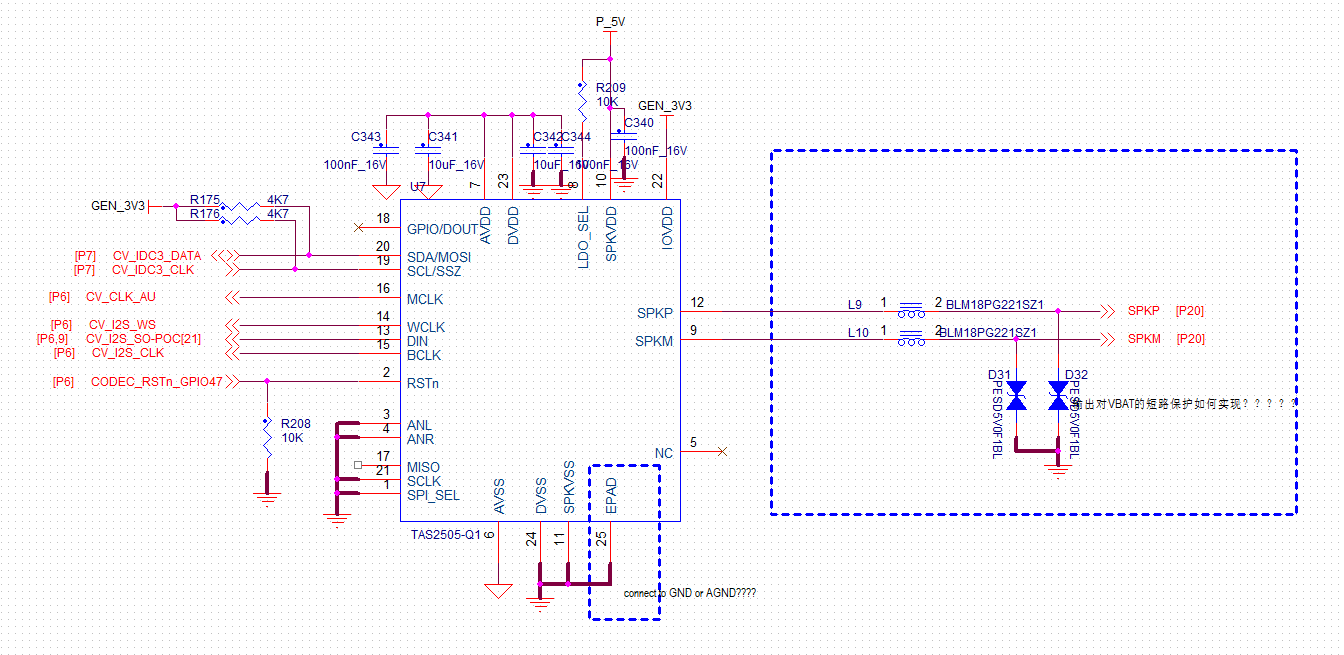
1. Is thermal pad of PIN connected to GND or AGND?

2. The specifications mention shutdown power consumption. But it's not clear how to get into shutdown mode, just pull down RST?

3. Are there any corrections to the following circuit ?

Thank you

Jerry
  • Hi Jerry,

    Below are some comments on your questions:
    1. You could use the pad below the IC as star connection for AGND and GND, you should connect the pad to the GND plane that provides the best heat dissipation. I'll confirm tomorrow the relation between *VSS pins and the pad.
    2. Pulling RST down should provide low power consumption. If you want to enable low power without resetting the device, you could disable the Class-D driver, PLL, DAC and analog blocks by register writes. Perhaps the easiest is to pull RST down and then re-initialize the device.
    3. You should add decoupling caps for IOVDD as you do for AVDD and DVDD. Please make sure that AINx are never enabled, if you think these could be enabled at some point you could add capacitors to GND to prevent any bias at the input pins from shorting to GND. Or you can also short AINx pins together as explained in data sheet Layout Guidelines.

    Best regards,
    -Ivan Salazar
    Applications Engineer - Low Power Audio & Actuators
  • Hi Ivan

    Thank you very much.

    Jerry
  • Jerry,

    Just a follow-up comment. There is no internal connection between the pad and *VSS pins, so it is OK to connect it either to AGND or GND. There is still the suggestion to use the pad as star connection for grounds and also connect it to the best heat dissipating plane.

    Best regards,
    -Ivan Salazar
    Applications Engineer - Low Power Audio & Actuators