This thread has been locked.

If you have a related question, please click the "Ask a related question" button in the top right corner. The newly created question will be automatically linked to this question.

TAS5766M: Smart Amp exchanges I2S data with master, but no analog audio appears on DAC output

Part Number: TAS5766M


Can someone help me resolve an issue with the TAS5766M SmartAmp we can’t seem to get around in our new custom design?

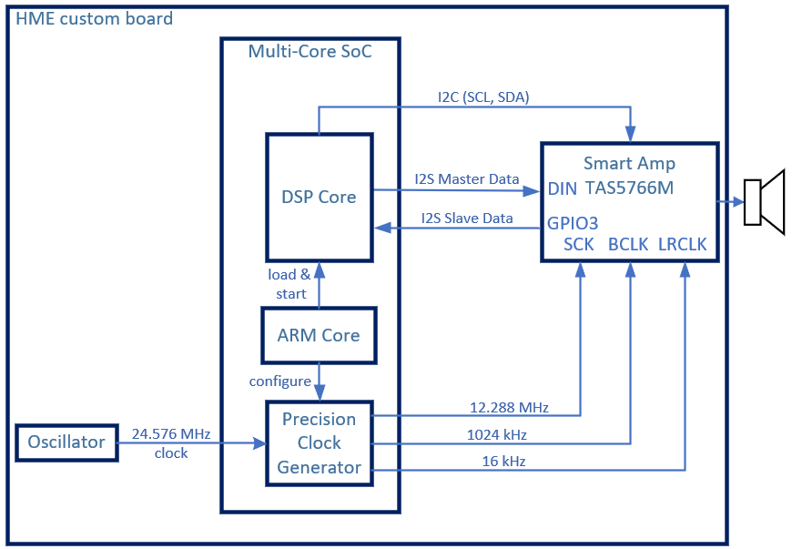
In this new design, we’ve connected the SmartAmp’s SCK input to a Precision Clock Generator (PCG) block output on our DSP, so the SmartAmp doesn’t have a SCK upon power-up until this DSP configures its PCG to provide a 12.288 MHz clock (along with 1024 kHz BCK and 16 kHz LRCK clocks) from a 24.576 MHz external oscillator. We’ve found that the SmartAmp must be sent into power-down mode by setting the I2C page 0 register 2 bit 0, clearing it, and delaying 10 ms to see any I2S data come out from the SmartAmp’s SDOUT (via GPIO3) signal. However, even with this SDOUT data coming from the input to the DAC, we don’t see any modulation of the power amp’s OUTPR/L signals because the INPR (cap-connected DACR) signal is at a constant DC level (biased at 3.3V). The problem seems to be the DAC isn't converting the audio samples at its input (as SDOUT shows) to an analog input signal to the Smart Amp's built-in power amp to modulate an (observed) 768 kHz PWM signal at (which just looks like high voltage 50% duty cycle clock).

Any suggestions appreciated.

  • At this point, I don't see anything else I can do but try to get any analog audio signal to get past the DAC & come out of the Smart Amp on our custom board by using the PurePath Console (PPC3) app. Can someone confirm that I can use the PPC3 app connected to my custom target board through a Total Phase Aardvark I2C-to-USB Host Adapter?

  • Tried connecting the 24.576 MHz oscillator available on power-up directly into TAS5766M's SCK input, instead of 12.288 MHz that starts-up later. No difference in the TAS5766M's behavior: I2S data traffic flows in both directions but no DAC output signal (constant 0 VDC) feeding into built-in power amp (INPR).  Collected some scope captures & register contents after a few thousand samples sent over I2S (see below). Also tried to route some internal signals to GPIO2, giving the following results:

       Page 0 / Register 82 (Hex 0x52)   GPIO2 Output Selection

       These bits select the signal to output to GPIO2. To actually output the selected signal, the GPIO2 must be set to output mode at Page 0 / Register 8.

           Default value: 0000

           0000: off (low)  -->   constant 0V

           0001: DSP GPIO2 output  -->  constant 0V

           0010: Register GPIO2 output (Page 0 / Register 86, bit 2)    -->  sometimes toggled for debugging purposes

           0011: Auto mute flag (asserted when both L and R channels are auto muted)  -->  constant 0V

           0100: Auto mute flag for left channel   -->  constant 0V

           0101: Auto mute flag for right channel   -->   constant 0V

           0110: Clock invalid flag (clock error or clock changing or clock missing)   -->   constant 0V

           0111: Serial audio interface data output (SDOUT)    -->  GPIO3/SDOUT as labelled "DOUT from SA" in scope captures

          1000: Analog mute flag for left channel (low active)   constant ~3.3V

          1001: Analog mute flag for right channel (low active)   constant ~3.3V

          1010: PLL lock flag   -->  constant ~3.3V

          1011: Charge pump clock    -->  1.536 MHz square wave

          1100: DAC clock    -->  6.14 MHz square wave, not sure if 6.14 MHz clock ( = 6 x 1024 kHz BCLK) is correct for DAC

          1101: MiniDSP clock/4    -->   4.10 MHz square wave, not sure if 16.4 MHz clock is correct for miniDSP

          1110: Under voltage flag, asserted when XSMUTE voltage is higher than 0.7 DVDD   -->   constant ~3.3V  ????

          1111: Under voltage flag, asserted when XSMUTE voltage is higher than 0.3 DVDD    -->  constant ~3.3V  ????

  • did you check power on sequence follow datasheet figure32? also could you share your setup pictures to us review? did this TAS5766 play with TI EVM or customer board?
  • As I've said in my original problem description when I opened the case, we know the power-on sequence of Figure 32 is not met because our design connects the TAS5766M's I2S clock inputs to Precision Clock Generator (PCG) block outputs on our DSP, so it doesn’t have SCK, BCK or LRCK upon power-up, but rather not until after the DSP runs to the point it configures its PCG to provide a 12.288 MHz SCK (along with 1024 kHz BCK and 16 kHz LRCK) from a 24.576 MHz external oscillator. We expected to be able to reset the TAS5766M at that point, if it need it.

    Taking the TAS5766M into powerdown mode & back out into standby mode has been sufficient to get the TAS5766M to send I2S data (DAC input) back to our DSP on SDOUT/GPIO3, but that restart sequence doesn't seem to allow the DAC to take that input we see on SDOUT/GPIO3 and convert it to an analog signal for the internal amplifier.

    Hoped my description was sufficient to give you a clear understanding of what we're doing, but here's a picture of it if it helps.

  • Actually, when I say "we know the power-on sequence of Figure 32 is not met", I should add that we've connected the 24.576 MHz oscillator output directly to the TAS5766M SCK so it does have a (faster) clock on power-up, and it doesn't appear to change the DAC output. So, for some other reason, the DAC is not converting samples to an analog waveform on DACR . Somehow, it appears muted, but we can't find any indication in status or control registers that it is. By the way, our configuration is using a single speaker, as described in section 8.2.2 "Mono/PBTL Application" on page 44 of the manual.
  • See additional details I provided above, as requested.

  • Hi Jean,

    How is the TAS5766M device in your design initialized?  Do you feed 4-wire I2S signals (SCLK, BCLK, LRCLK, and DATA) to TAS5766M?

    A Total Phase Aardvark I2C-to-USB Host Adapter is not necessary and also it doesn't work with PPC3 GUI.

    Try the In-System Tuning mode instead.

    Andy

  • Andy,

    Yes, as my original description & the diagram I posted afterward describe, our system provides a common 12.288 MHz master clock to all audio devices on the board, along with a 1024 kHz bit clock and a 16 kHz L/R channel clock to send I2S data to, and receive I2S data from each device.All devices (except input-only devices like microphones which obviously dont have data going to them) have these 5 signals connected. Like my original description says, per your datasheet's Figure 43 "Example Process Flow" on page 32 shows, we've verified there's sample data coming back on GPIO3 (SDOUT) (see the scope capture I provided earlier) so the DAC has data at its input but nothing is coming out of DACR. Again, we're using the TAS5766M in mono mode, just like the datasheet's section 8.2.2 "Mono/PBTL Application" on page 44 describes.  So, my question remains; **** Why is the DACR output at a constant 0V when the DAC inputs show data going to it on both left & right channels, when all the registers I've dumped & the scope outputs don't show any problem aside form the SOF error? ****  Please look at both of these I posted earlier (above) and answer that straight forward question. 

    Thank you for confirming that the Total Phase Aardvark I2C-to-USB Host Adapter will not work with PPC3 GUI.

  • Hi Jean,

    I will take care of this issue offline and therefore I will close this e2e thread.

    Andy