This thread has been locked.

If you have a related question, please click the "Ask a related question" button in the top right corner. The newly created question will be automatically linked to this question.

SRC4392: None of RX ports working, only Port A and B and TX output

Part Number: SRC4392
Other Parts Discussed in Thread: SN74LVC1G125

Hello everybody,

I'm trying to get the SRC4392 to work properly on my design. Using port A and or B as slave ports there is no problem to get them on TX output, coax and optical. Even passtrought from A to B I2S works.

There is a microcontroller that controls all the I2C stuff for the SRC4392, unfortunately, I'm stuck somewhere with the inputs. There is no way to make them work, neither doing a DIR-DIT bypass. I tried to follow some forum explanations on the init code, but no luck. This is my init routine:

# set register page to 0 (Control and Status Registers)
bus.write_byte_data(address, 0x7f, 0x00)

# port A setup as slave with I2S data format
bus.write_byte_data(address, 0x03, 0x01)
bus.write_byte_data(address, 0x04, 0x00)

# port B setup as master with I2S data format, SRC as data source, MCLK as clock source, clock divider 128
bus.write_byte_data(address, 0x05, 0x39)
bus.write_byte_data(address, 0x06, 0x00)

# DIR setup using MCLK, set to mute audio for loss of lock condition, RXCKO disabled
# Default input is RX1
bus.write_byte_data(address, 0x0d, 0x08)
bus.write_byte_data(address, 0x0e, 0x00)

# PLL1 setup for 24.576MHz P=2 J=8 D=0
bus.write_byte_data(address, 0x0f, 0x22)
bus.write_byte_data(address, 0x10, 0x00)
bus.write_byte_data(address, 0x11, 0x00)

# set GPO1 to enable 22.5792 Clock
bus.write_byte_data(address, 0x1b, 0x01)

# set GPO2 to enable 24.576 Clock
bus.write_byte_data(address, 0x1c, 0x01)

# set GPO3 to use MCLK 24.576 (set to 0x00 to use 22.5792)
bus.write_byte_data(address, 0x1d, 0x01)

# set GPO4 to use RXCKI 24.576 (set to 0x00 to use 22.5792)
bus.write_byte_data(address, 0x1e, 0x01)

# SRC setup is default with port A as the input data source
# MCLK is the ref clock source, AUTODEM enabled (use 0x2d, 0x02 to play audio from the S/PDIF coax input and 0x00 for PORT A I2S)
bus.write_byte_data(address, 0x2d, 0x02)
bus.write_byte_data(address, 0x2e, 0x20)
bus.write_byte_data(address, 0x2f, 0x00)

# DIT setup with the SRC as the input data source and MCLK as master clock
# clock divider is 128 to set the output frame rate
# block start is an output and valid audio is indicated
# c and u data will not be updated
bus.write_byte_data(address, 0x07, 0x1c)
bus.write_byte_data(address, 0x08, 0x00)
bus.write_byte_data(address, 0x09, 0x00)

# set left channel colume -3.5dB
bus.write_byte_data(address, 0x30, 0x07)

# set right channel colume -3.5dB
bus.write_byte_data(address, 0x31, 0x07)

# power up all blocks
bus.write_byte_data(address, 0x01, 0x3f)

I also tried to add this at the end of the init file:

# DIT setup for 192KHz
bus.write_byte_data(address, 0x07, 0x1c)

bus.write_byte_data(address, 0x08, 0x08)
bus.write_byte_data(address, 0x7f, 0x02)
bus.write_byte_data(address, 0x2e, 0xee)
bus.write_byte_data(address, 0x2f, 0xff)
bus.write_byte_data(address, 0x7f, 0x00)
bus.write_byte_data(address, 0x08, 0x00)
bus.write_byte_data(address, 0x7f, 0x02)
bus.write_byte_data(address, 0x2e, 0x01)
bus.write_byte_data(address, 0x2f, 0x01)
bus.write_byte_data(address, 0x7f, 0x00)

# Reset
bus.write_byte_data(address, 0x01, 0x80)

But no luck, only works when selecting input from Port A or B. Audio input sample rate is the same as used on MCLK and RXCKI clocks, so should work.. but nothing.

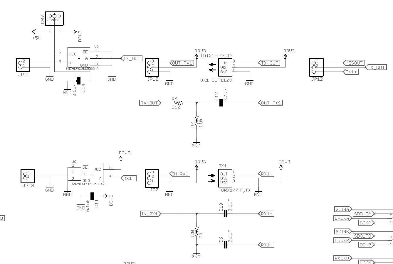
This is my input/output schematic, just in case there's something wrong.. (I don't think so anyway):

I also have another question regarding sample rate input detection. My design has two clocks for 44.1 and 48 sample rate frequencies. I can switch them separately on/off and use one or another separately for MCLK and RXCKI. How can I aut-detect the input sample rate to switch between RXCKI 22.5792 or 24.576 clock?

Thanks!
Oriol.

  • Hi Oriol,
    Thanks for providing the detailed init code in addition to the other details. I'll review the same and see what the possible disconnect is...Thanks.

    Best regards,
    Ravi
  • Hi Oriol,
    i have used the below script for BYPASS mode on the EVM and you can refer to this for bypass mode. Will also share the DIR->SRC->DIT scripts as well.

    # set register page to 0
    w e0 7f 00
    # dit line driver and aesout outputs use bypass mux as data source
    # rx1 input selected by bypass mux
    w e0 08 30
    # power up the dir block
    w e0 01 22

    # rx2 input selected by bypass mux
    w e0 08 70

    # rx3 input selected by bypass mux
    w e0 08 b0

    # rx4 input selected by bypass mux
    w e0 08 f0

    # rx1 input selected by bypass mux
    w e0 08 30


    Best regards,
    Ravi
  • This is the other script that can be referenced as well. This is for DIR->SRC->DIT routing -
    w e0 7f 00
    # dir setup is default with audio muted for loss of lock condition and rxcko enabled
    w e0 0d 00
    w e0 0e 09
    # pll1 setup for 24.576mhz rxcki p is 2 j is 8 d is 0
    w e0 0f 22
    w e0 10 00
    w e0 11 00
    # set gpo1 for dir nonaudio flag
    w e0 1b 06
    # set gpo2 for dir nonvalid flag
    w e0 1c 07
    # set gpo3 for dir emphasis flag
    w e0 1d 05
    # set gpo4 for dir parity error flag
    w e0 1e 0d
    # src setup is default with the dir as the input data source
    # mclk is the ref clock source
    w e0 2d 02
    w e0 2e 00
    w e0 2f 00
    w e0 30 00
    w e0 31 00
    # dit setup with the src as the input data source and mclk as master clock
    # mclk divider is 512 to set the output frame rate
    # block start is an output and valid audio is indicated
    # c and u data is sourced from the data buffers in register page 2
    w e0 07 7c
    w e0 08 00
    w e0 09 01
    # power up all blocks except port a and b
    w e0 01 27
    # disable dit buffer transfers
    w e0 08 08
    # set register page to 2
    w e0 7f 02
    # set dit channel status data for bytes 0 thru 2
    # professional use pcm audio no emphasis locked 48khz sampling freq
    # all other channel status bytes are set to default 0x00 value
    w e0 00 81
    w e0 01 81
    w e0 02 10
    w e0 03 10
    w e0 04 34
    w e0 05 34
    # set register page to 0
    w e0 7f 00
    # enable dit buffer transfers
    w e0 08 00

    # dit setup for 96k output
    w e0 07 3c
    w e0 08 08
    w e0 7f 02
    w e0 00 80
    w e0 01 80
    w e0 08 08
    w e0 09 08
    w e0 7f 00
    w e0 08 00
  • To what is the DIR output routed?
    Can you use a 'scope to check the state of the LOCK output on pin 11?

    As for indicating the input sample rate: if the SRC is the destination for the DIR, then you can use the SRC Ratio Readback registers to tell you the SRC ratio, and if you know the SRC output rate, then the input frequency can be easily determined.

    But, is there really a need to change the DIR reference clock? Use a 24.576 MHz reference clock for the DIR and leave it.
  • Dear Andy,

    You are right, I had on my mind that I needed to use two different clocks for different input sample rates on DIR, but actually not. Using 24.576Mhz works for 44.1 and 48kHz sample rates. Actually only need to change it for DIT output sample rate. I think I missunderstood something on the datasheet.

    Lock pin, RDY, and INT are connected to Microcontroller so I can easily read them in any case. But actually found the problem, the buffer used for TTL input was forcing low the optical input, really weird... after desoldering buffer, works like a charm..  It's really strange this happens, to me my schematic looks good.

    Thank you so much for your support!

    Oriol.

  • Dear Ravi,

    This actually works, thank you! But actually found the real problem, the buffer used for TTL input was forcing low the optical input, really weird... after desoldering buffer, works like a charm.. It's really strange this happens, to me my schematic looks good.

    I need to use both TTL and optical inputs at "same" time, that tmeans that user no needs to use jumpers or something similar. Any help on this?

    Thank you so much for your support!

    Oriol.
  • Okay one more thing here! Related to clocks.. What if I want to switch between I2S Port A input and RX inputs? For RX inputs 24.576 is perfect, but if I play a file via I2S at 44.1kHz, this does not work, only at 44.1kHz, that's why I need to switch to the 22.5792 clock.

    So actually my question about detecting input sample rate was about this. Any suggestion?

    Thanks!
    Oriol.
  • "I need to use both TTL and optical inputs at "same" time, that tmeans that user no needs to use jumpers or something similar. Any help on this?"

    Basically, you can't. Only on RX input can be decoded at a time.

    There is a mux that selects which RX input drives the AES3 decoder. The DIR can decode only one input at a time. The output of the DIR can feed the SRC, the DIT or either of the Audio Serial Ports (I2S). For this to work, though, your design has to select the desired input. It cannot autodetect which input to use. Consider two valid AES streams on two of the RX inputs -- how can the chip decide? So at the least you need to provide a user interface which lets your user choose which RX input to use, and based on that choice you program register 0x0D Receiver Control Register 1.

    Now, there is the Bypass Mux, which lets you select any of the four RX inputs to drive the AES and TX± outputs directly without going through the AES decoder and encoder. But this of course means you can't use the TX output for anything other than that direct input.

  • "So actually my question about detecting input sample rate was about this. Any suggestion?"

    You can use the SRC's rate estimator for this. The rate estimator looks at the selected SRC source (port A, port B or DIR) output and uses the selected SRC reference clock to determine that source's sample rate. The RDY flag is asserted when that rate estimation is complete and you can read the SRI and SRF registers to get that estimate.
  • Dear Andy,

    Thank you so much for your response. Unfortunately I think you have not understood correctly my question, or probably I was not so clear explaining the situation!

    The design has 4 optical inputs, that also allows to use coax if user wants to use it instead of optical input. So coax and optical shares same RX input, of course! User obviously cannot connect Optical and Coax at same time, I just want to give the user the possibility to use the one he/she wants.

    So, in addition, there are four TTL inputs, that user can also use in case don't want to use Optical or Coaxial. Or just because the user requeriment matches using TTL inputs.

    Now the problem here relays that TTL buffer is forcing low the RX inputs, so that's why I was not able to get Optical and Coax inputs working. When desoldered buffers from the board, inputs start to work. 

    So just asking why I'm having this behaviour on the buffer, because there's should be no problem at all with that (you can check my design above with input buffers). Input is floating, bout output shoudn't be forced to zero, isn't it? I'm stuck here!

    Thank you!

  • "You can use the SRC's rate estimator for this. The rate estimator looks at the selected SRC source (port A, port B or DIR) output and uses the selected SRC reference clock to determine that source's sample rate. The RDY flag is asserted when that rate estimation is complete and you can read the SRI and SRF registers to get that estimate."

    Also regarding this, it should work the same way as DIR? I mean, using only one clock frequency I'm able to re-sample all input sample rates, 44.1 and 48kHz ones, without the need to change to specific sample rate clock. Port A and B should work the same way? Because as far as I see I need to switch from one clock to another to play files using I2S signals on Port A and B, doesn't work the same way as DIR. But this change also makes me change all the init setup everytime user uses a diferent sample rate. So I do not have a clear idea of how actually the SRC works here.

    Also if I want to re-sample to 88.2kHz for example, instead 96kHz, I can still use the 24,576 clock? As far as I know I need to switch to the 22.5792 one. That's why I do not understand correctly this part, because DIR can accept any sampling rate using only one clock, but DIT not?

    Sorry for all those questions but is not so clear on the datasheet! Will be nice to have also some help from TI staff.

    Thank you so much!
    Oriol.
  • What is this TTL buffer?
  • I'm using the SN74LV1G125. Output is always enabled in order to bring it easier to the user, just conect ttl or not. If not using TTL then just plug optical or Coax. I know that is High Z output if output is not enabled, but if it's enabled and input is floating? Shouldn't be output too?

    Thanks!
    Oriol.
  • "I know that is High Z output if output is not enabled, but if it's enabled and input is floating? Shouldn't be output too?"

    From the SN74LVC1G125 data sheet, page 12, section 12.1 Layout Guidelines: "All unused inputs of digital logic devices must be connected to a high or low bias to prevent them from floating."

    In other words, never let a CMOS input float. This advice goes back to the beginning of time. A weak pull-down or pull-up resistor, something easily overcome by a connected driver, should be put on the input if there is ever a chance that the input will be undriven.
  • Andy Peters said:
    "I know that is High Z output if output is not enabled, but if it's enabled and input is floating? Shouldn't be output too?"

    From the SN74LVC1G125 data sheet, page 12, section 12.1 Layout Guidelines: "All unused inputs of digital logic devices must be connected to a high or low bias to prevent them from floating."

    In other words, never let a CMOS input float. This advice goes back to the beginning of time. A weak pull-down or pull-up resistor, something easily overcome by a connected driver, should be put on the input if there is ever a chance that the input will be undriven.

    Thank you Andy,

    I will solve this issue using more buffers in combination of 125 and 126, so when one is enabled the other one is disabled, this way will cause no troubles between TTL and Optical/Coax inputs.

    What about my other question?

    Oriol said:

    Also regarding this, it should work the same way as DIR? I mean, using only one clock frequency I'm able to re-sample all input sample rates, 44.1 and 48kHz ones, without the need to change to specific sample rate clock. Port A and B should work the same way? Because as far as I see I need to switch from one clock to another to play files using I2S signals on Port A and B, doesn't work the same way as DIR. But this change also makes me change all the init setup everytime user uses a diferent sample rate. So I do not have a clear idea of how actually the SRC works here.

    Also if I want to re-sample to 88.2kHz for example, instead 96kHz, I can still use the 24,576 clock? As far as I know I need to switch to the 22.5792 one. That's why I do not understand correctly this part, because DIR can accept any sampling rate using only one clock, but DIT not?

    Thank you so much!

    Oriol.

  • Can anybody help me please?

    Running SRC4392 in I2S slave mode only plays 48kHz sample rates files, even using the 22.5792 clock as reference. Why? I'm stuck on this!

    Thank you,

    Oriol.

  • Ok now I see where the problem is.. files at 44.1kHz with BCLK 2.8MHz are working perfectly, files at 44.1kHz and BCLK 1.4MHz not. Suggestions?

    Thanks!
  • What generates the BCLK? 1.4 MHz is not correct for 44.1 kHz sampling -- it should be 2.822 MHz.