This thread has been locked.

If you have a related question, please click the "Ask a related question" button in the top right corner. The newly created question will be automatically linked to this question.

TLV320DAC3203: Dual DMIC support

Part Number: TLV320DAC3203

Hi Team,

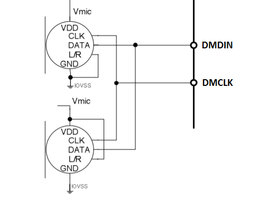
We try to TLV320DAC3203 support dual DMIC. Is it ok as below block diagram?

How to communicate these two DMIC without data conflict?

Thanks

  • Hi, Daniel,

    The block diagram is correct. Both left and right digital microphones must share the clock and data lines. You would only need to enable one microphone for left data operation and the other for right data operation as shown in the diagram below:

    I'm also attaching an example script for the digital microphone connection with the TLV320DAC3203. This script configures the TLV320DAC3203 to send the digital microphone data to the DOUT pin and to the headphone driver outputs (HPR / HPL).

    ###############################################
    # Digital Microphone Script Loopback
    # ---------------------------------------------
    # Digital microphone data (DOUT) is sent to
    # the DAC's DIN pin internally. DOUT data
    # is also sent to the USB controller.
    ###############################################


    ###############################################
    # Software Reset
    ###############################################
    #
    # Select Page 0
    w 30 00 00
    #
    # Initialize the device through software reset
    w 30 01 01
    #
    ###############################################


    ###############################################
    # Clock and Interface Settings
    # ---------------------------------------------
    # The codec receives: MCLK = 11.2896 MHz,
    # WCLK = 44.1 kHz
    ###############################################
    #
    # Select Page 0
    w 30 00 00
    #
    # PLL_clkin = MCLK, codec_clkin = PLL_CLK,
    # PLL on, P=1, R=1, J=8, D=0000
    w 30 04 03 91 08 00 00
    #
    # NDAC = 2, MDAC = 8, dividers powered on
    w 30 0b 82 88
    #
    # DOSR = 128
    w 30 0D 00 80
    #
    # NADC = 2, MADC = 16, dividers powered on
    w 30 12 82 90
    #
    # AOSR = 64
    w 30 14 40
    #
    # Digital Loopback
    # Routes DOUT to DIN internally, DOUT pin
    # is still output, DIN pin is ignored
    w 30 1D 10
    #
    ###############################################


    ###############################################
    # Configure Power Supplies
    ###############################################
    #
    # Select Page 1
    w 30 00 01
    #
    # Disable weak AVDD in presence of external
    # AVDD supply
    w 30 01 08
    #
    # Enable Master Analog Power Control
    w 30 02 00
    #
    # Set the input power-up time to 3.1ms (for ADC)
    w 30 47 32
    #
    # Set the REF charging time to 40ms
    w 30 7b 01
    #
    ###############################################


    ###############################################
    # Configure Processing Blocks
    ###############################################
    #
    # Select Page 0
    w 30 00 00
    #
    # PRB_P2 and PRB_R2 selected
    w 30 3C 02 02
    #
    ################################################
    # High-pass first order Butterworth2 filter,
    # fc = 80 Hz
    ###############################################
    #
    # Write to Buffer A:
    #
    # BIQUAD A, Left Channel (Page 8, Register 36, C7-C11)
    w 30 00 08
    w 30 24 7E F8 EB 00 81 07 15 00 7E F8 EB 00 7E F7 DD 00 82 0C 0C 00
    #
    # BIQUAD A, Right Channel (Page 9, Register 44, C39-C43)
    w 30 00 09
    w 30 2c 7E F8 EB 00 81 07 15 00 7E F8 EB 00 7E F7 DD 00 82 0C 0C 00
    #
    # Write to Buffer B:
    #
    # BIQUAD A, Left Channel (Page 26, Register 36, C7-C11)
    w 30 00 1A
    w 30 24 7E F8 EB 00 81 07 15 00 7E F8 EB 00 7E F7 DD 00 82 0C 0C 00
    #
    # BIQUAD A, Right Channel (Page 27, Register 44, C39-C43)
    w 30 00 1B
    w 30 2c 7E F8 EB 00 81 07 15 00 7E F8 EB 00 7E F7 DD 00 82 0C 0C 00
    #
    ###############################################


    ###############################################
    # Configure ADC Channel
    ###############################################
    #
    # Select Page 0
    w 30 00 00
    #
    # Configure MISO as clock output for DIGMIC
    w 30 37 0E
    #
    # LADC and RADC enabled for DIGMIC
    # Route SCLK as DIGMIC_DATA
    # Power up LADC/RADC
    w 30 51 DC
    #
    # Unmute LADC/RADC
    w 30 52 00
    #
    ###############################################


    ###############################################
    # Configure DAC Channel
    ###############################################
    #
    # Select Page 1
    w 30 00 01
    #
    # De-pop: 5 time constants, 6k resistance
    w 30 14 25
    #
    # Route LDAC/RDAC to HPL/HPR
    w 30 0c 08 08
    #
    # Select Page 0
    w 30 00 00
    #
    # DAC => 0dB
    w 30 41 00 00
    #
    # Power up LDAC/RDAC
    w 30 3f d6
    #
    # Select Page 1
    w 30 00 01
    #
    # Unmute HPL/HPR driver, 0dB Gain
    w 30 10 00 00
    #
    # Power up HPL/HPR
    w 30 09 30
    #
    # Select Page 0
    w 30 00 00
    #
    # Unmute LDAC/RDAC
    w 30 40 00
    #
    ###############################################
    

    I hope this helps you. Please let me know if you have more questions or comments.

    Best regards,
    Luis Fernando Rodríguez S.