Other Parts Discussed in Thread: TLV320AIC3100
Hello,
Our customer is facing issue of little bit older device that TLV320AIC10.
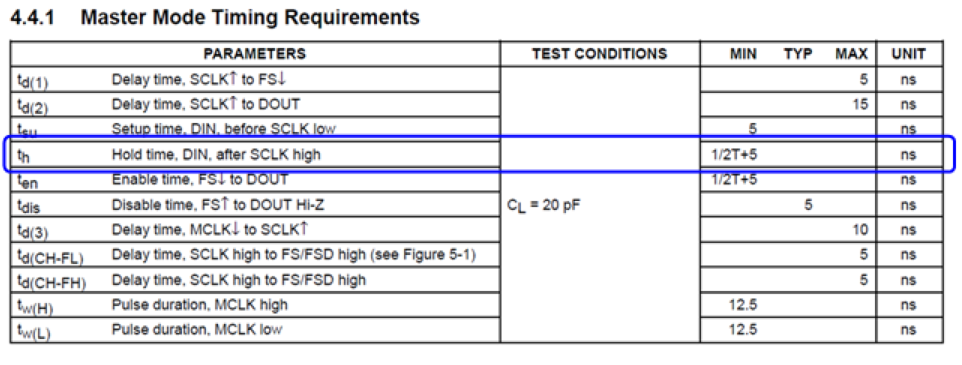
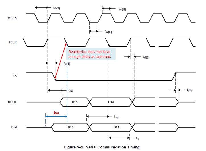
In Master mode, AIC10 generate SCLK and FS clocks. However those output clocks will violated DAC Data input setup time requirement itself.
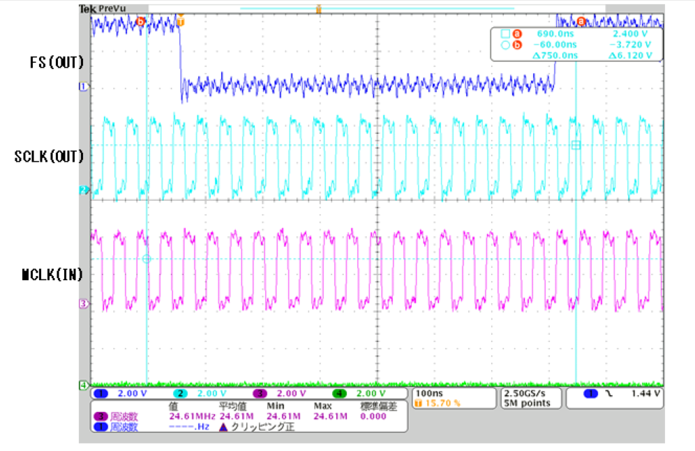
Here is the mode setting and input MCLK frequency.
M1=1 M0=1 M/S=1 Frame-Sync (FS) Function—Master Mode
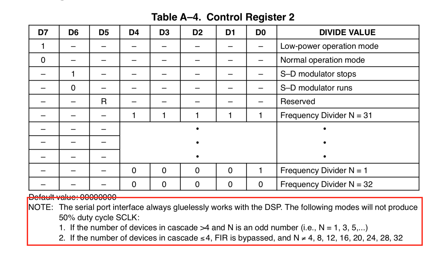
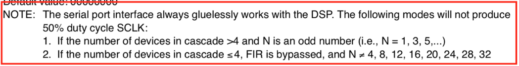
Register1=0x04(decimation/FIR Bypass)
Register2=0x06(N=6)
Register3=0x01(16-bit data format)
Register4=0x00(DAC PGA gain=0dB)
MCLK=19.6608MHz
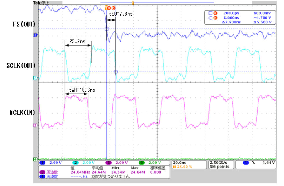
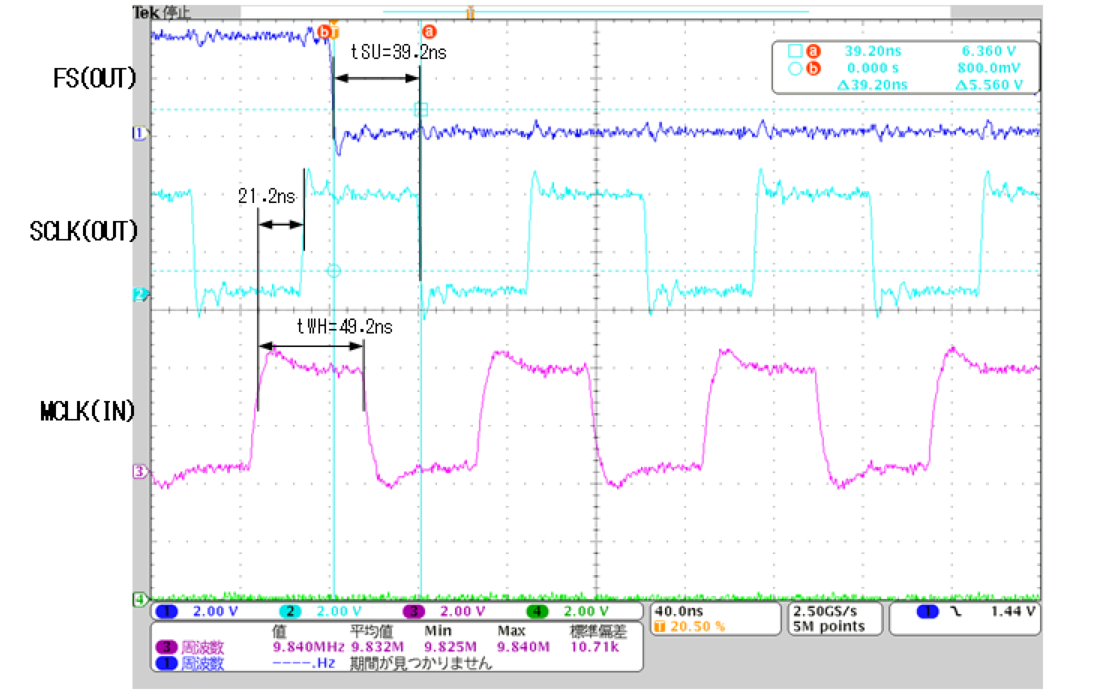
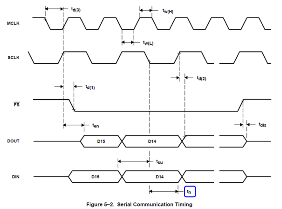
Captured waveform are followings.
Because of this FS-SCLK timing violation our DSP cannot catch appropriate 1st SCLK falling edge to output 16bit MSB data to DAC and violate tsu requirement.
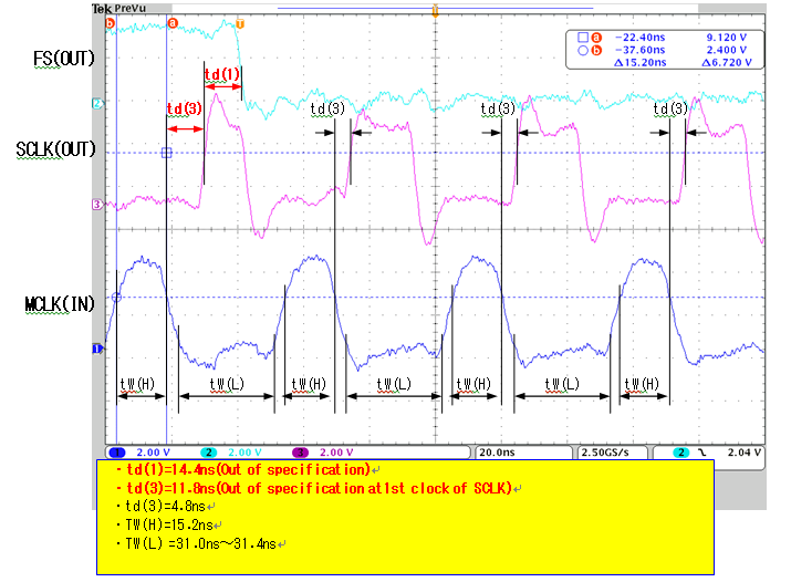
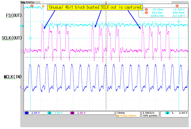
Q1:It seems SCLK clock is 4bit block busted output, it is unusual SCLK format, normally Audio converter SCLK output is continues clock. Is it correct function of AIC10 internal clock divider ?
Q2: Is there any good solution to keep Setup time tSU 5nsec(mini) requirement for DAC Data input when we use this very narrow FS falling edge to SCLK falling edge clock timings from master mode AIC10 generated?
Regards,
Mochizuki