This thread has been locked.

If you have a related question, please click the "Ask a related question" button in the top right corner. The newly created question will be automatically linked to this question.

TPA3128D2: PLIMIT questions

Part Number: TPA3128D2
Other Parts Discussed in Thread: TPA3132D2,

Is there any way to determine the PLIMIT voltage required other than experimentally?  Some of the other parts with PLIMIT have graphs showing PLIMIT vs Max. Output Power,
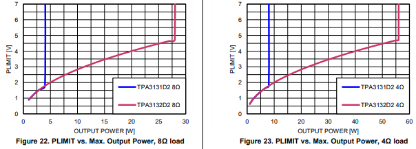
but the TPA3128D2 only states "The "virtual" rail is approximately four times the voltage at the PLIMIT pin" and Table 3 indicates the ratio of PLIMIT voltage (V) to Output Voltage (Vrms) ranges from 12.67/3.3=3.84 to 6.3/1.5=4.2.  Are the units on this table correct with the output voltage Vrms, because he text says the 4x is for Vpeak?

Is GVDD as loosely regulated as the datasheet indicates (5.1V 5.6V 6.3V)?  This would translate to a power limit range of -17% to +27% if the nominal GVDD is used for calculations.

In section 6.5 DC Electrical Characteristics,

Does this indicate that the limit may kick in 32% (1-(6.75/8.2)^2) below the nominal power level
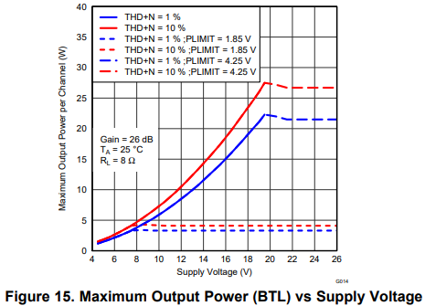
 when the PLIMIT voltage is set precisely?  Is this range related to the VCC?  The TPA3132D2 datasheet has graphs indicating higher clip levels when the virtual rails are close to the actual supply voltage.
My desire is to design an amplifier using the TPA3128D2 which runs off a higher than needed VCC (24V) and limit the maximum unclipped output power to a guaranteed level (15W).  Is this feasible?  If I am interpreting the datasheet correctly for G, GVDD, and Vo , I would need to set the PLIMIT at 33W (15/(0.89 * 5.1/5.6 * 6.75/8.2)^2)to guarantee 15W if I use GVDD or 29W (15/(0.89 * 0.99 * 6.75/8.2)^2) if I use a 1% voltage reference.  These number do not seem reasonable.

Thanks in advance for your assistance in clarifying the PLIMIT operation.

Jon

  • Hi Jon,

    1) The OUTPUT VOLTAGE (Vrms)  of Table 3 in TPA3128 datasheet is typo. It is peak-peak value, not RMS value.

    2) The "virtual" rail is approximately four times the voltage at the PLIMIT pin. That is not very accurate. Because the GVDD has some range and the PCB trace, the connection cable also have power loss. The divided resistors also have tolerance.

    3) The unclipped power calculation is not considered to connection cable power loss. In actual application, the power loss should be considered.

    4)  We suggest you can verify the PLIMIT on EVM board according to you user case and cable connection firstly. If you have no EVM board, I can help you.

  • Thank you for the quick response.

    1. OK

    2. If I use a more tightly regulated supply to generate the PLIMIT voltage, are the tolerances tighter?

    3. The power losses in the cables, inductors, PCB traces, connectors, etc. are very small compared to the tolerances.  My design will take these into account.

    4. What portion of the tolerances are internal to the TPA3128D2?  If I use an external precision voltage source for PLIMIT (after experimentally determining the value), how much variation in the clip level will I see unit-to-unit in production?  For instance, Table 3 states a PLIMIT of 3.3V will create a "virtual" rail of Vp=12.67V.  Using RL=8 and Rs=0.018 gives Pout=9.94W.  What is the tolerance range on the 12.67V (or Pout) assuming an ideal PLIMIT voltage?

  • Hi Jon,

    The tolerance is mainly from the TPA3128 internal circuit, not from the power on PLIMIT pin. So if you use external supply on PLIMIT pin can not fix the tolerance. I have confirmed with designer, the internal tolerance maybe 20% at worst. So we suggest that consider the margin on your design.

    Derek,

    Regards

  • Derek,

    Thank you again.

    Can you clarify if the 20% tolerance is on the clipping voltage (Vp) or on power (Pout)?  +/-20% on Vp becomes  +44%/-36% on Pout.

  • Hi Jon,

    Yes. So we suggest that you can verify on EVM boards under your using case.

    Thanks!

    Derek,

    Regards