This thread has been locked.

If you have a related question, please click the "Ask a related question" button in the top right corner. The newly created question will be automatically linked to this question.

TAS5411-Q1: Mute and enable sequence problem

Part Number: TAS5411-Q1

Dear team,

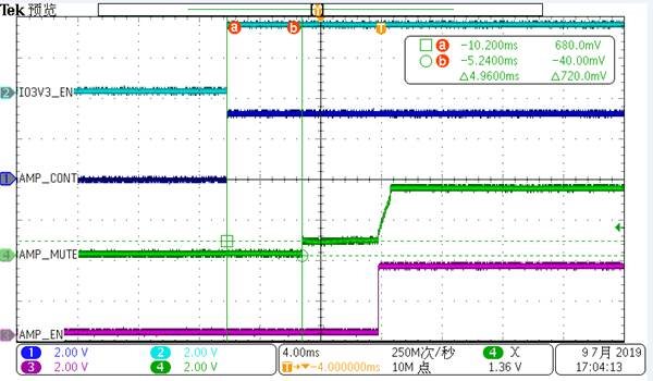
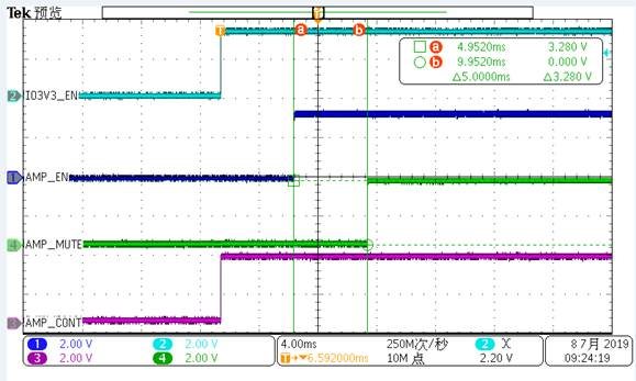
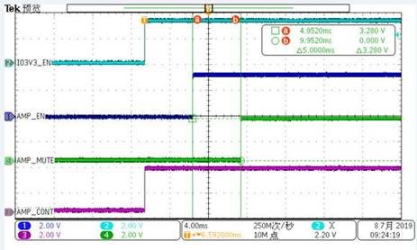
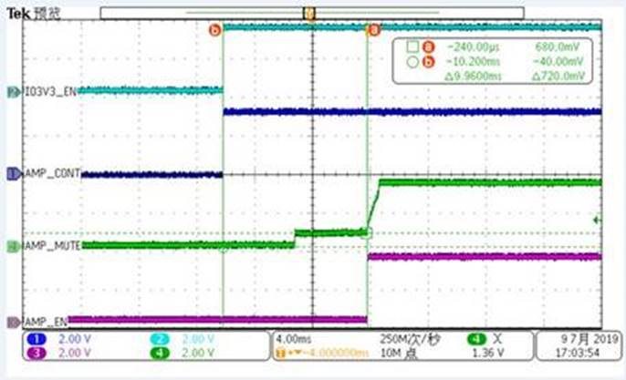
When we actually test the MUTE pin, if MUTE is pulled high before STANDBY (the AMP_EN in the figure below), the intermediate level voltage will appear. If MUTE is pulled high after STANDBY, the intermediate level voltage will not appear. Could you please help explain the reason? Is it the effect of internal circuits?
Can the MUTE pin recognize such an intermediate level voltage?

Thanks & Best Regards,

Sherry

  • Sherry,

    We recommend the first scenario and your scope plot is correct.  The mid level of the MUTE is accurate when the /STANDBY pin is low.  This is internal circuitry making this occur.  This is normal for this device..

  • Hi Gregg,

    Whether the mid level of the MUTE will impact the MUTE pin or the IC? Does this mid level have the minimum and maximum? Could you please help explain why the mid level exist? And what effect will they have on the chip and the MUTE pin?

    In addition, the second scenario is also working, right? Can we use this second scenario?

    Thanks & Best Regards,

    Sherry

  • Sherry,

    The MUTE pin on the TAS5421 is active high.  The device is muted when the MUTE pin is high and unmuted when low.  The AMP_MUTE signal is inverted in your plots.  Maybe that is why there is confusion on the first plot.  Please advise on the AMP_MUTE signal.

  • Sherry,

    Any update on this?  If not, I will close the thread.

  • Hi Gregg,

    My customer's application is that the device mute when working normally, and when the system has an unmute request, the device will un-mute. So the power on sequence for my customer is PVDD, MUTE, and then release standby as below, but under this sequence, there is always a mid level voltage existing. The value of the mid level voltage is sometimes 0.6V, or sometimes 2.2V , and this value is not fixed. I hope MUTE pin pull up before releasing the Standby pin, in this way, we can avoid the pop sound. But because this mid level voltage is not fixed, when the voltage is larger, the device is in mute mode, but when the voltage is smaller, the device will be in un-mute mode. So if I can't control the sequence between the mute pin and standby pin. Then how should  I do?

    Best Regards,

    Sherry

  • Hi Sherry,

    I understand better and now I can explain what is happening on the MUTE pin. 

    When the TAS5411 is in STANDBY mode, the internal power supplies are off.  This allows for the MUTE pins "float".  When there is PVDD present and in STANDBY, there is a leakage path that pulls up on the MUTE pin.  This is normal and the voltage can be anything up to about 2.6Vdc.   It does not affect the operation of the device.

  • Hi Gregg,

    Thanks for your reply!

    When the standby change form 0 to 1 or 1 to 0, there will be a small pop sound, if at this time this device is in mute mode, this pop sound will be avoided, but if this device is in um-mute mode, the pop sound will be magnified which can be heard by our ear. In order to avoid the pop sound, I hope when the standby changes, the device is in mute mode. So I hope the mute pin pull up firstly, and then release the standby. But as we can see, if the device is in standby mode, the mute can't be pulled up. Then how do we solve the pop sound problem?

    Thanks & Best Regards,

    Sherry

  • Sherry,

    I need a schematic.  I will take this offline now, since this is a customer's schematic.