Other Parts Discussed in Thread: TPA3005D2
Hi,
We use TLV320AIC3254 with 16kHz sample rate on our products.
And we would like to modify the current 16kHz design to 192kHz sample rate for new production.
We set the PLL as below (using MCLK=16MHz) via PurePath Studio based on the section 2.7.1 of the ARG.
They meets the PLL clock range and also (PLL_CLKIN/P) condition.
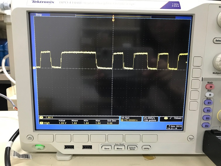
But it does not work.
reg[ 0][ 5] = 0x91 ; P=1, R=1, J=5
reg[ 0][ 6] = 0x05 ; P=1, R=1, J=5
reg[ 0][ 7] = 0x0e ; D=3760
reg[ 0][ 8] = 0xb0 ; D=3760
reg[ 0][ 4] = 0x03 ; PLL_clkin = MCLK, codec_clkin = PLL_CLK, PLL on
reg[ 0][254] = 0x0a ; Delay 10ms for PLL to lock
reg[ 0][ 12] = 0x87 ; MDAC = 7, divider powered on
reg[ 0][ 13] = 0x00 ; DOSR = 32(MSB)
reg[ 0][ 14] = 0x20 ; DOSR = 32(LSB)
reg[ 0][ 18] = 0x87 ; NADC = 7, divider powered on
reg[ 0][ 19] = 0x82 ; MADC = 2, divider powered on
reg[ 0][ 20] = 0x20 ; AOSR = 32
reg[ 0][ 11] = 0x82 ; NDAC = 2, divider powered on
reg[ 0][ 27] = 0x0C ; Change MCLK-> input, BCLK, WCLK, output to FPGA
reg[ 0][ 26] = 0x81 ; Powerup WCLK output module
reg[ 0][ 30] = 0x84 ; Powerup BCLK output module and
reg[ 0][ 33] = 0x00 ; set WCLK source to ADC_FS
Do you have any other consideration about settings?
And could you give me the advice how to decide BCLK divider "N" value?
If that helps, we use TLV320AIC3254 for our current production with the following settings (MCLK=16MHz). It works well.
reg[ 0][ 5] = 0xD1 ; P=5, R=1, J=32
reg[ 0][ 6] = 0x20 ; P=5, R=1, J=32
reg[ 0][ 7] = 0x00 ; D=0000
reg[ 0][ 8] = 0x00 ; D=0000
reg[ 0][ 4] = 0x03 ; PLL_clkin = MCLK, codec_clkin = PLL_CLK, PLL on
reg[ 0][254] = 0x0a ; Delay 10ms for PLL to lock
reg[ 0][ 12] = 0x8A ; MDAC = 10, divider powered on
reg[ 0][ 13] = 0x00 ; DOSR = 128(MSB)
reg[ 0][ 14] = 0x80 ; DOSR = 128(LSB)
reg[ 0][ 18] = 0x85 ; NADC = 5, divider powered on
reg[ 0][ 19] = 0x8A ; MADC = 10, divider powered on
reg[ 0][ 20] = 0x80 ; AOSR = 128
reg[ 0][ 11] = 0x85 ; NDAC = 5, divider powered on
reg[ 0][ 27] = 0x0C ; Change MCLK-> input, BCLK, WCLK, output to FPGA
reg[ 0][ 26] = 0x81 ; Powerup WCLK output module
reg[ 0][ 30] = 0x90 ; Powerup BCLK output module and
reg[ 0][ 33] = 0x00 ; set WCLK source to ADC_FS
Best regards,