Part Number: TLV320ADC3100
Hi expert,
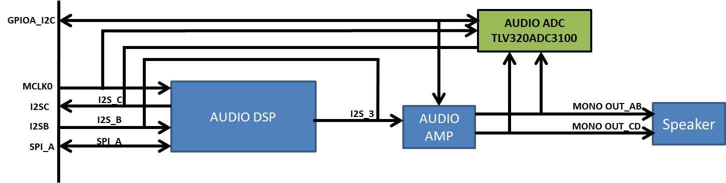
Could you help to check below circuit (Fig.1) connection is correct or not?
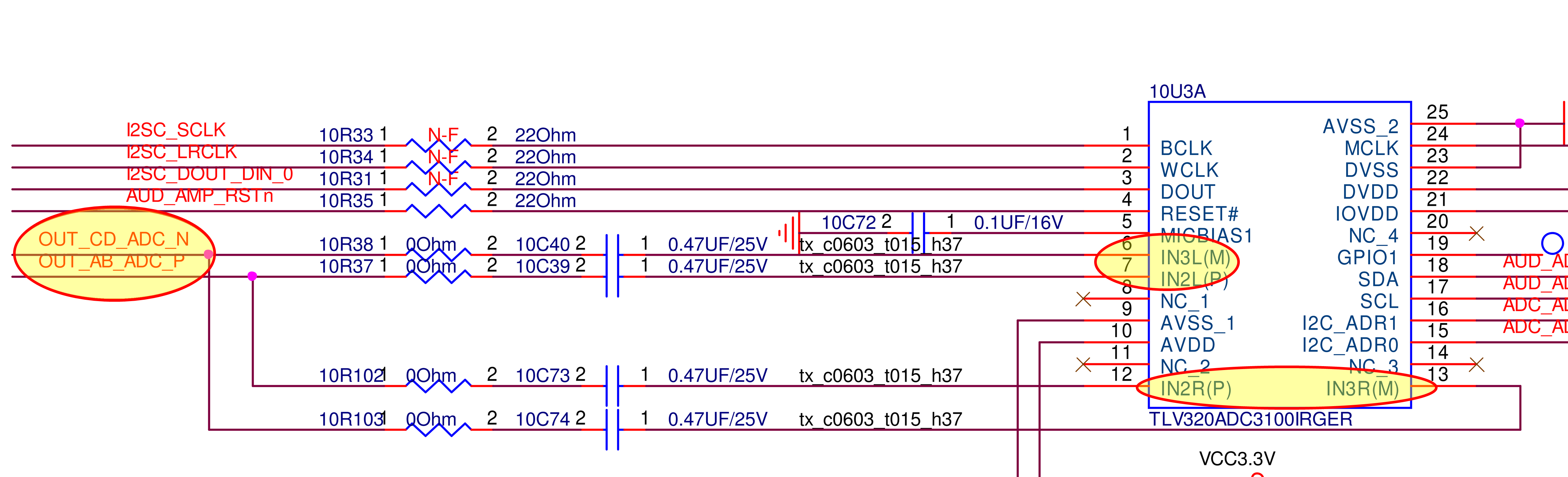
Fig.2 is the function block for you reference. The audio amp is a mono output with differential mode.
Fig.2 Function block
This thread has been locked.
If you have a related question, please click the "Ask a related question" button in the top right corner. The newly created question will be automatically linked to this question.
Part Number: TLV320ADC3100
Hi expert,
Could you help to check below circuit (Fig.1) connection is correct or not?
Fig.2 is the function block for you reference. The audio amp is a mono output with differential mode.
Fig.2 Function block
Teresa,
an unused micbias can be left floating, any unused input pins should be terminated with a 0.47uf capacitor to GND.
What kind of Audio levels are coming from the Audio Amplifier? I don't really see any attenuation circuit in the schematic you provided. I would assume that there is something like this somewhere? the full-scale input of the ADC3100 is 1.414Vrms differential, and the abs max is -0.3 -> AVDD+0.3V
I assume that the I2C pull-ups are elsewhere on the schematic.
Best regards,
-Steve Wilson
Teresa,
I don't see anything that I would consider "wrong" for a mono signal. it looks like they are connecting a differential output to a differential input, and that seems normal. I also suspect that they are using two channels so they could average the two channels and achieve +3dB SNR or for redundancy. The inputs they are using are the correct pins for each channel.
Because of the redundancy, and the 0 ohm resistors connecting the two channels I wasn't sure if there would ever be a case where the inputs were not used. IF there is a use case where 10R102 and 10R103 were not installed for example. it would be best of those inputs could be terminated.
best regards,
-Steve Wilson