This thread has been locked.

If you have a related question, please click the "Ask a related question" button in the top right corner. The newly created question will be automatically linked to this question.

PCM2912A: PCM2912A Schematic Review: Guitar Instrument Interface

Part Number: PCM2912A

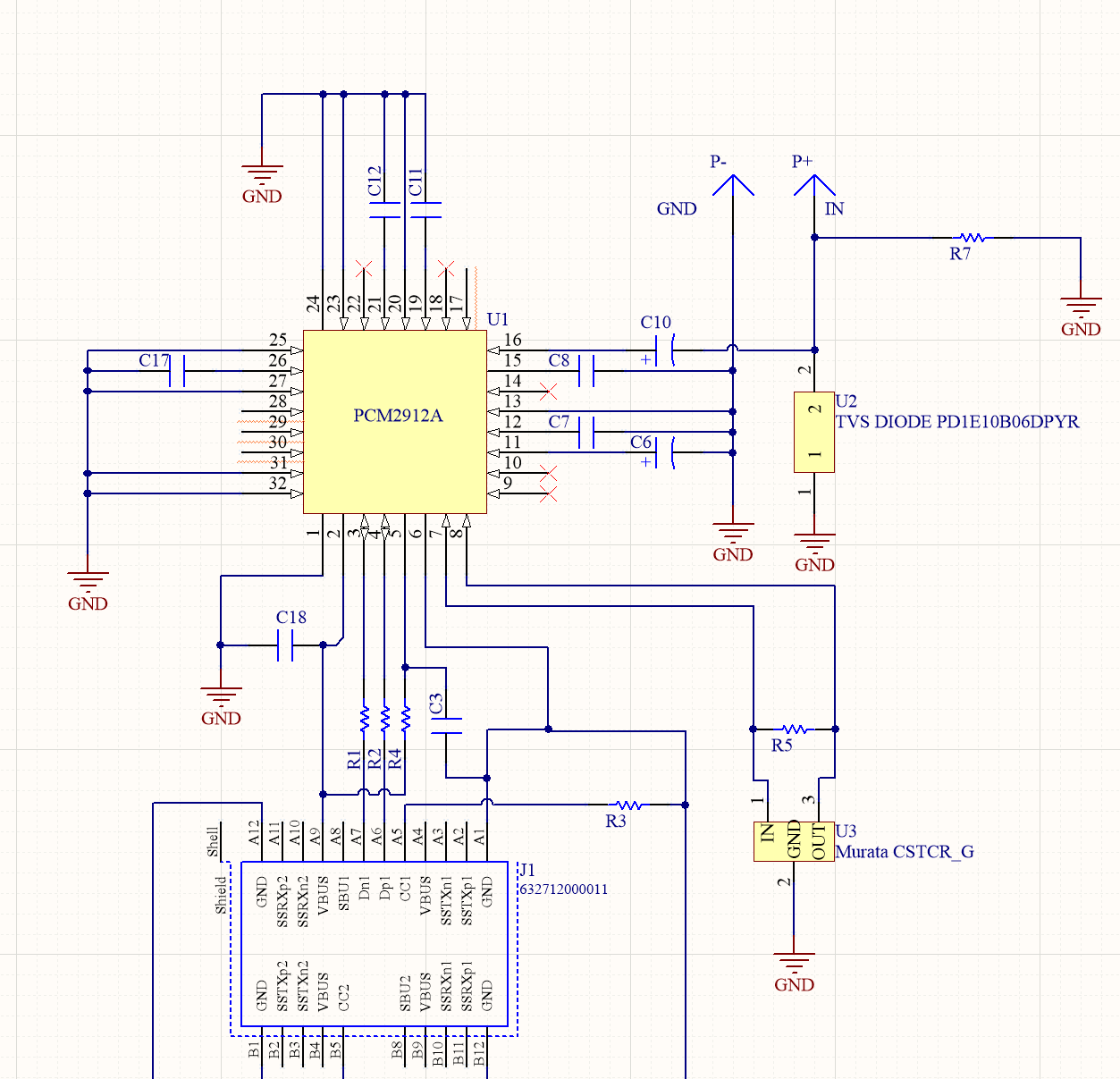
Hello, and thank you in advance for your assistance! I am writing to request a schematic design review for my application circuit utilizing the TI PCM2912A. The intended use case is to interface an electric guitar with a PC workstation via USB. The overall design has been copied from the DEM-PCM2912A EVM Schematic with some noted modifications which I would like feedback on:

  1. The output stage has been removed and replaced with the pin configuration described elsewhere in this forum. Pins 9,10,22,18 are floating; 21,19 coupled to GND via uF; 20 tied to GND
  2. A TVS diode (TI PD1E10B06DPYR) is included on the input stage to reduce risk of harmful transients when handling the plug. 
  3. This circuit uses a ceramic resonator (Murata CSTCR6M00G55-R0, with built in load caps) instead of a crystal with the intention of saving physical space on the board. I understand this may produce an undesirable noise level and am curious on any experience with this kind of part here. 
  4. This design uses a USB Type-C plug instead of Type-A, with CC1 and CC2 tied to GND indicating USB2.0 mode. 
  5. An input resistor (R7, 1Meg) is included to increase input impedance for the guitar instrument input. 
  6. PLAY and REC pins tied to GND (unused).

Do these design features appear correct and reasonable for the intended use case of maximizing SNR for the guitar input. 

Also, could you provide guidance on the proper configuration of the pins MUTE, nSSPND, MAMP, TEST0, TEST1?

Best

  • Hi Nate,

    I'm not familiar with USB-C but my understanding is that it is backwards compatible protocol wise so I don't foresee any issues with this. 

    The input resistor is not actually going to give you a 1Mohm input impedance because the mic input only has a 20kOhm input impedance and for AC you have effectively placed it in parallel with this. If you want a higher input impedance, you need to use a buffer.

    The PLAY and REC pins are outputs and should not be tied to ground. You should float them if you do not intend to use them.

    I'm not sure what you are asking regarding the other pins, you should refer to the datasheet for pin functionality.

    Best,

    Zak

  • Thanks, Zak. Any thoughts on the TVS? Specifically, if this would cause any performance issues?

  • Hey Nate,

    In general it's good practice to include protection components so it's good that you'e thinking of this. More often than not I see TVSs on a supply line and diode clamps to the supplies on the inputs, but that's certainly not the only way to protect the inputs. The main concern will be how you have selected your TVS, if the turn on is too early then you may have high leakage over some of your signal range and this could degrade linearity.

    We actually have a whole TI precision labs section on electrical overstress in data converters and how to protect the inputs. You might find this helpful: https://training.ti.com/node/1139109?context=1139747-1140267-1128375-1139109

    Best,

    Zak

  • Zak- do you have any data on the output capability of any of the other power pins (other than MBIAS)? I would consider using Vcca, Vdd, Vccp for the supply to a JFET buffer circuit in front of Vin, as you suggested. However, I am limited to MBIAS as that is the only output current characterized (2mA spec'd). Thanks

  • Hi Nate,

    I do not have any data on the sourcing capabilities of other pins, but I can say that these pins are provided purely for decoupling the internal regulators and are not intended to supply external circuits. MBIAS is the only pin that is designed for this purpose.

    Best,

    Zak