This thread has been locked.

If you have a related question, please click the "Ask a related question" button in the top right corner. The newly created question will be automatically linked to this question.

PCM1793: The left signal is not correct

Part Number: PCM1793
Other Parts Discussed in Thread: DIR9001, , LM833

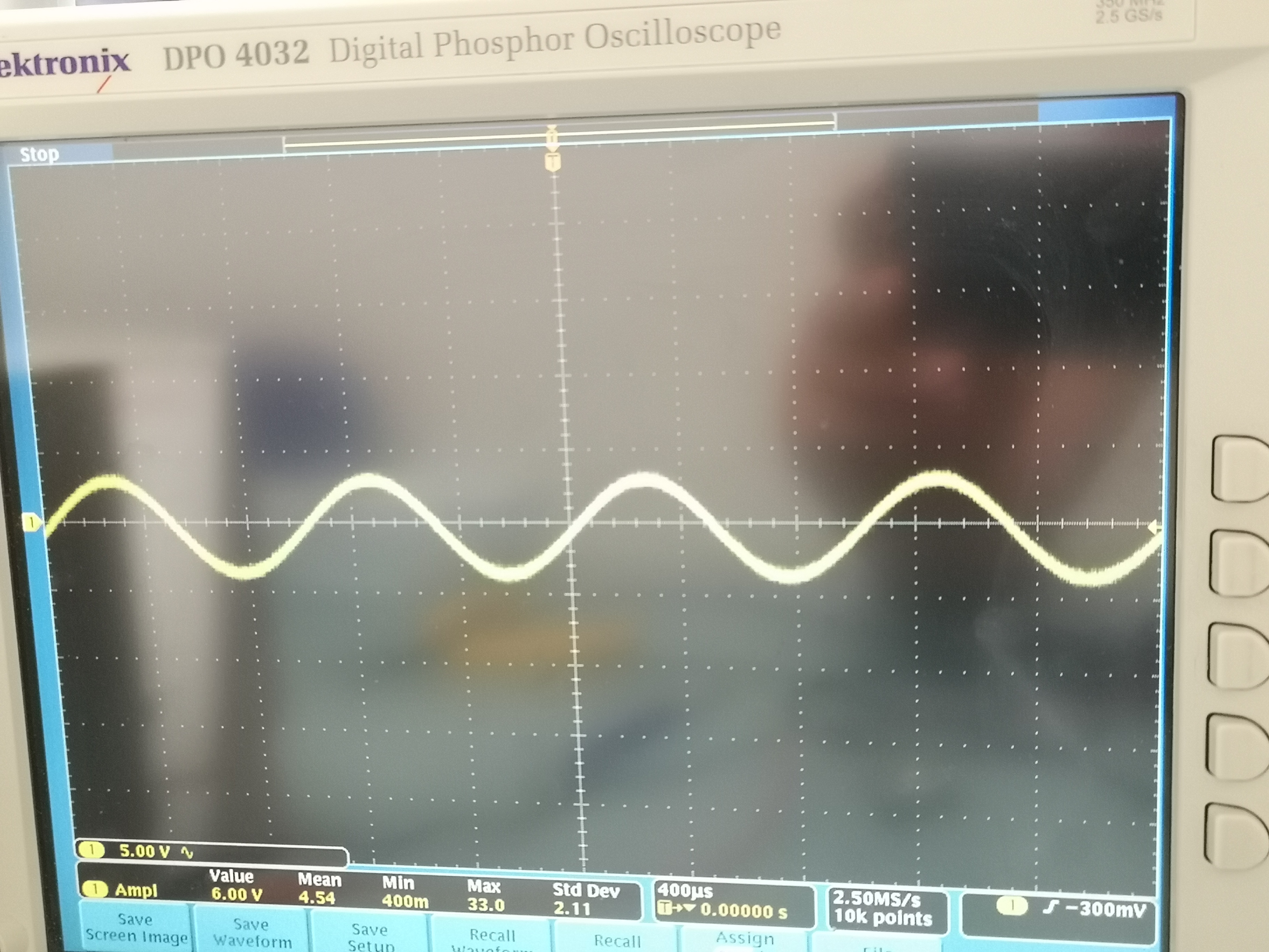
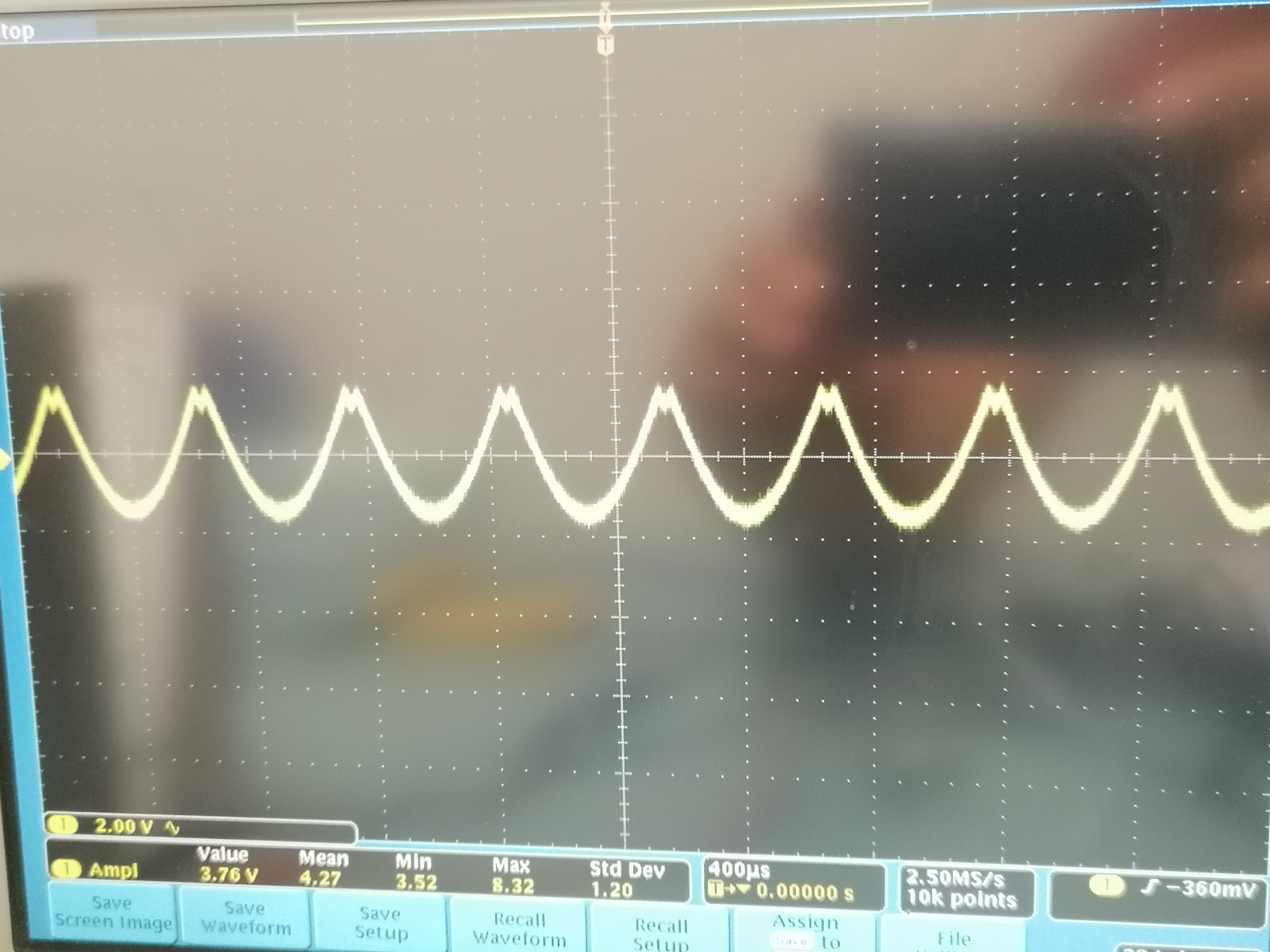
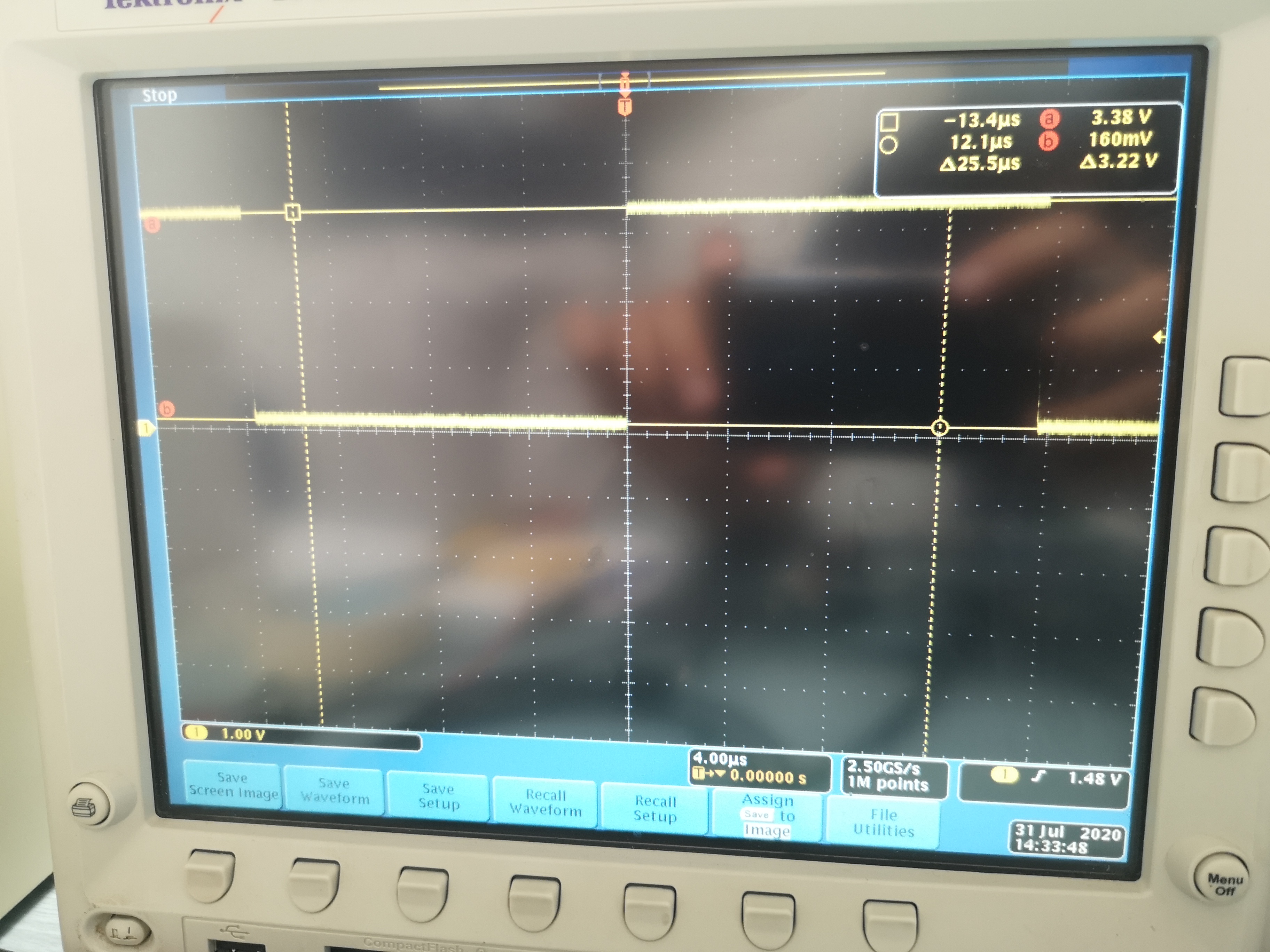
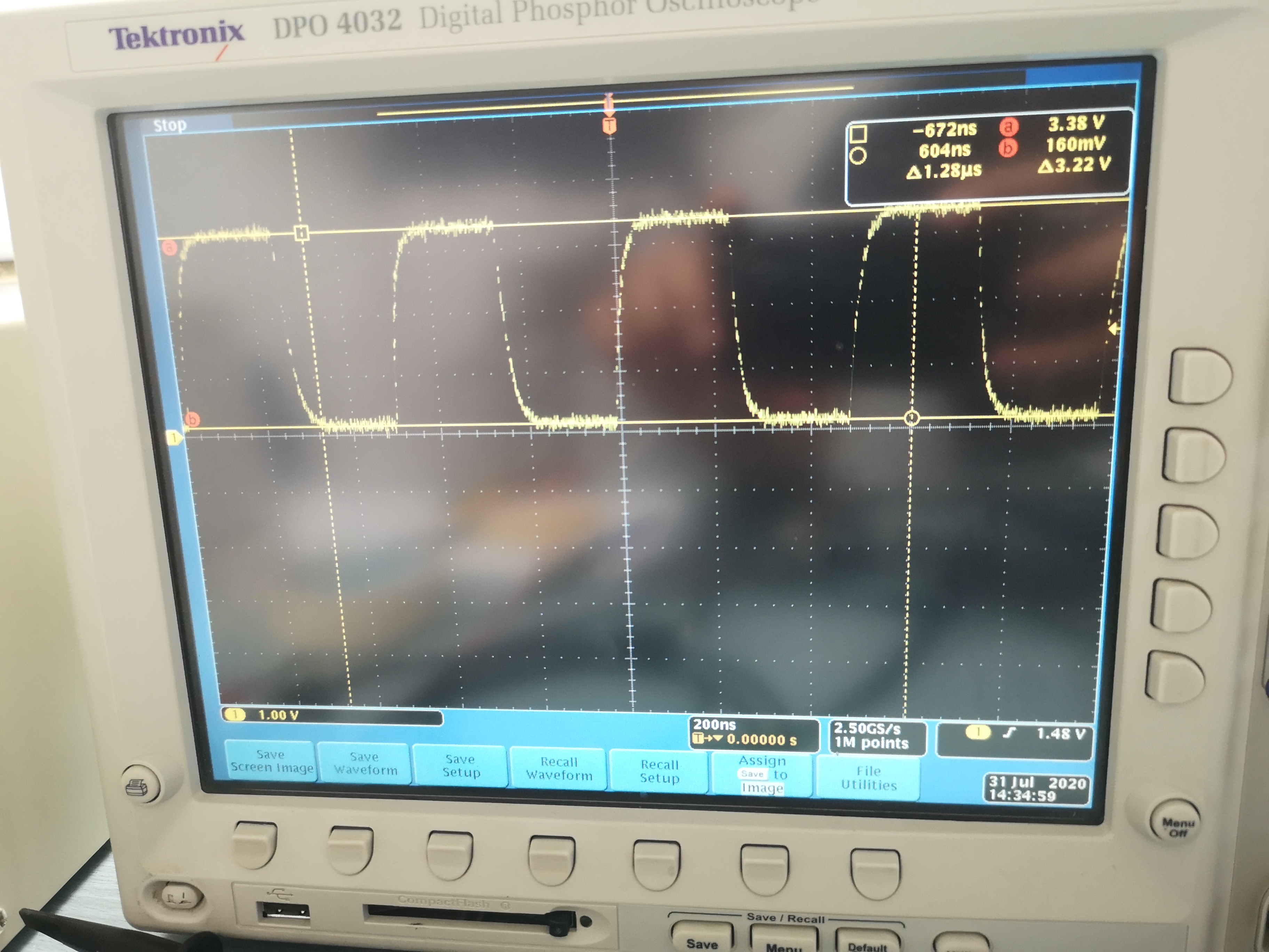
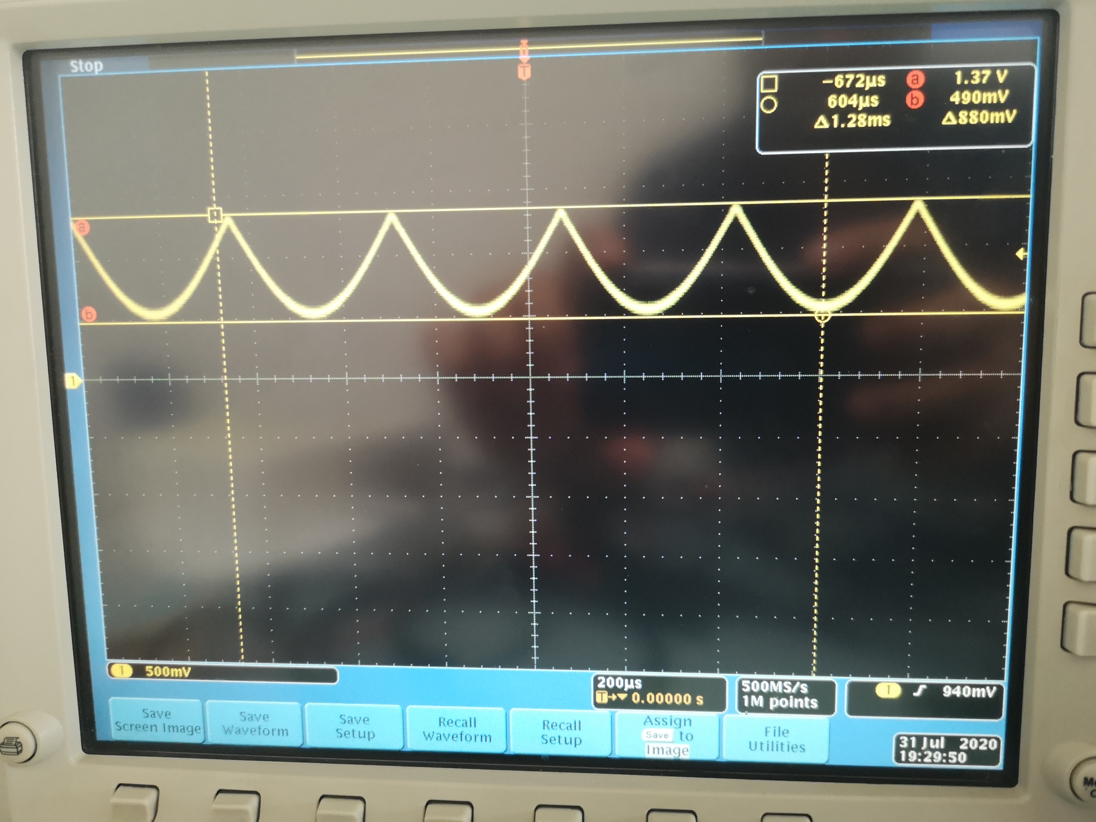
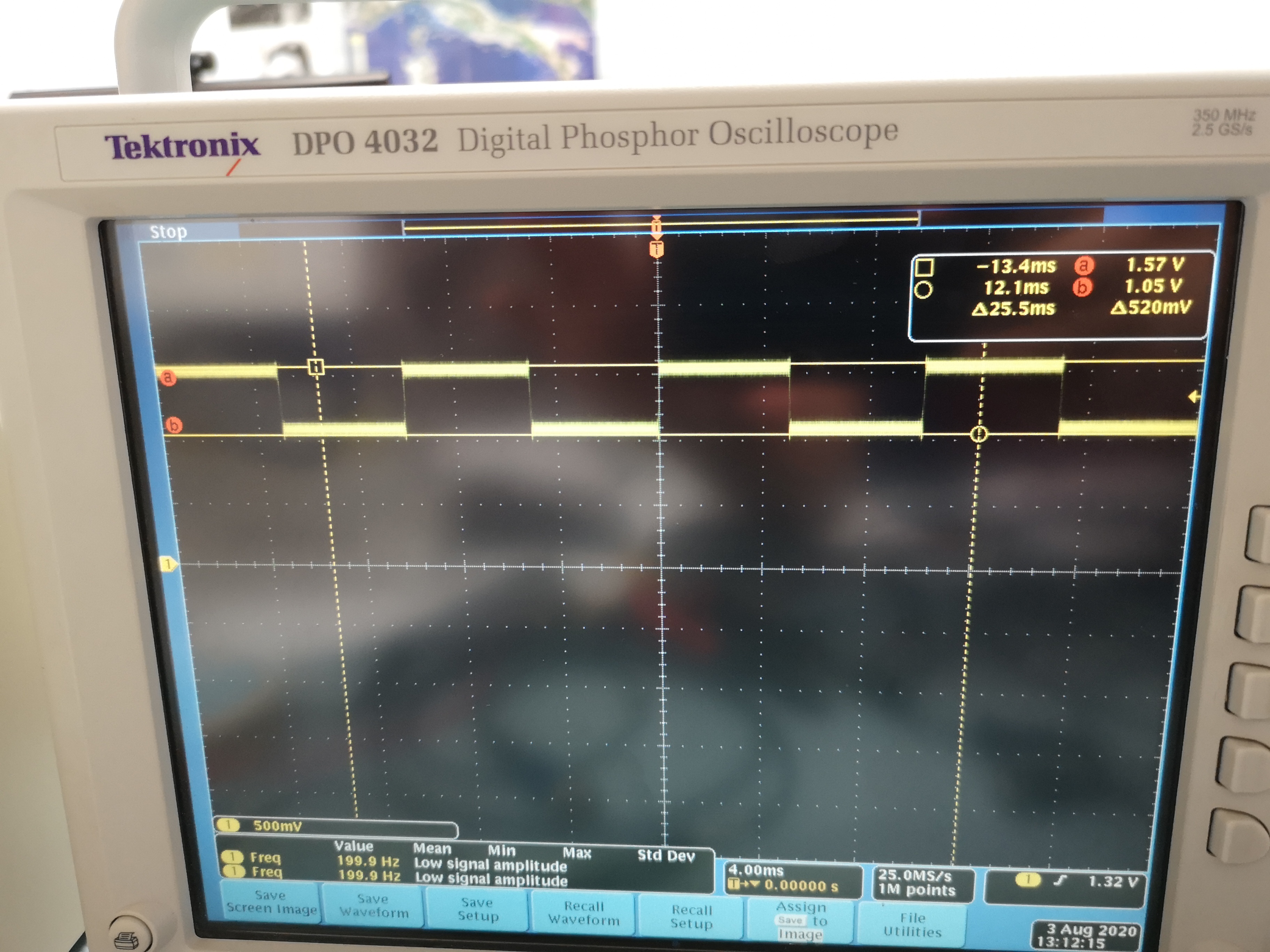
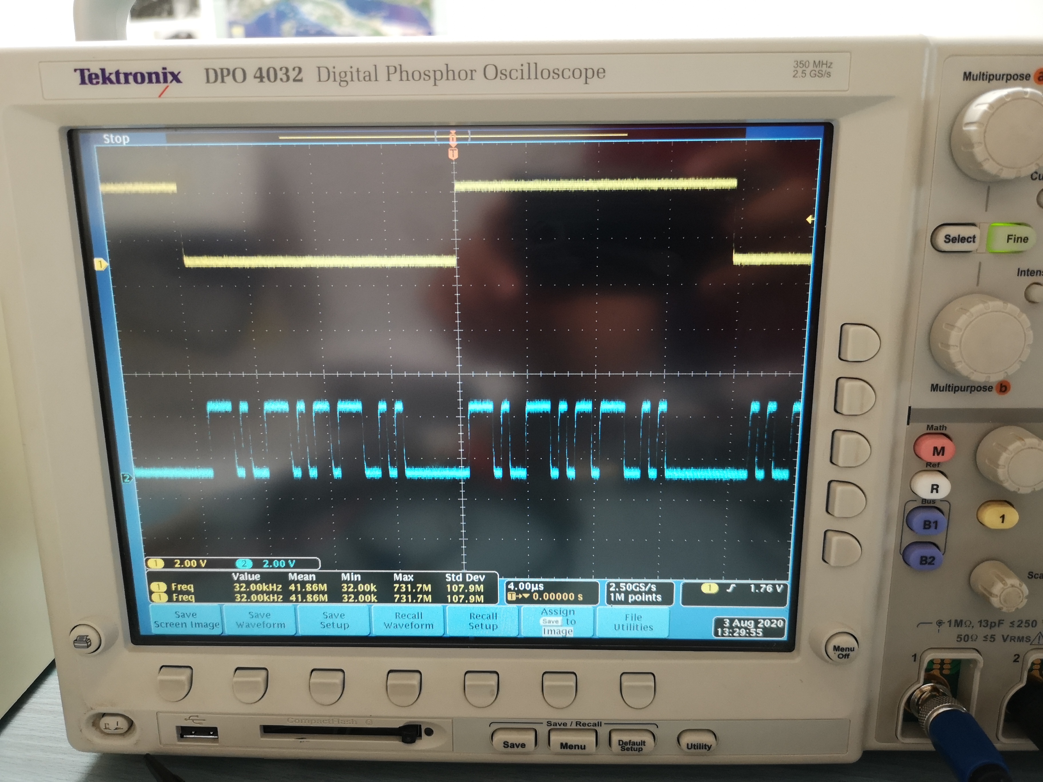
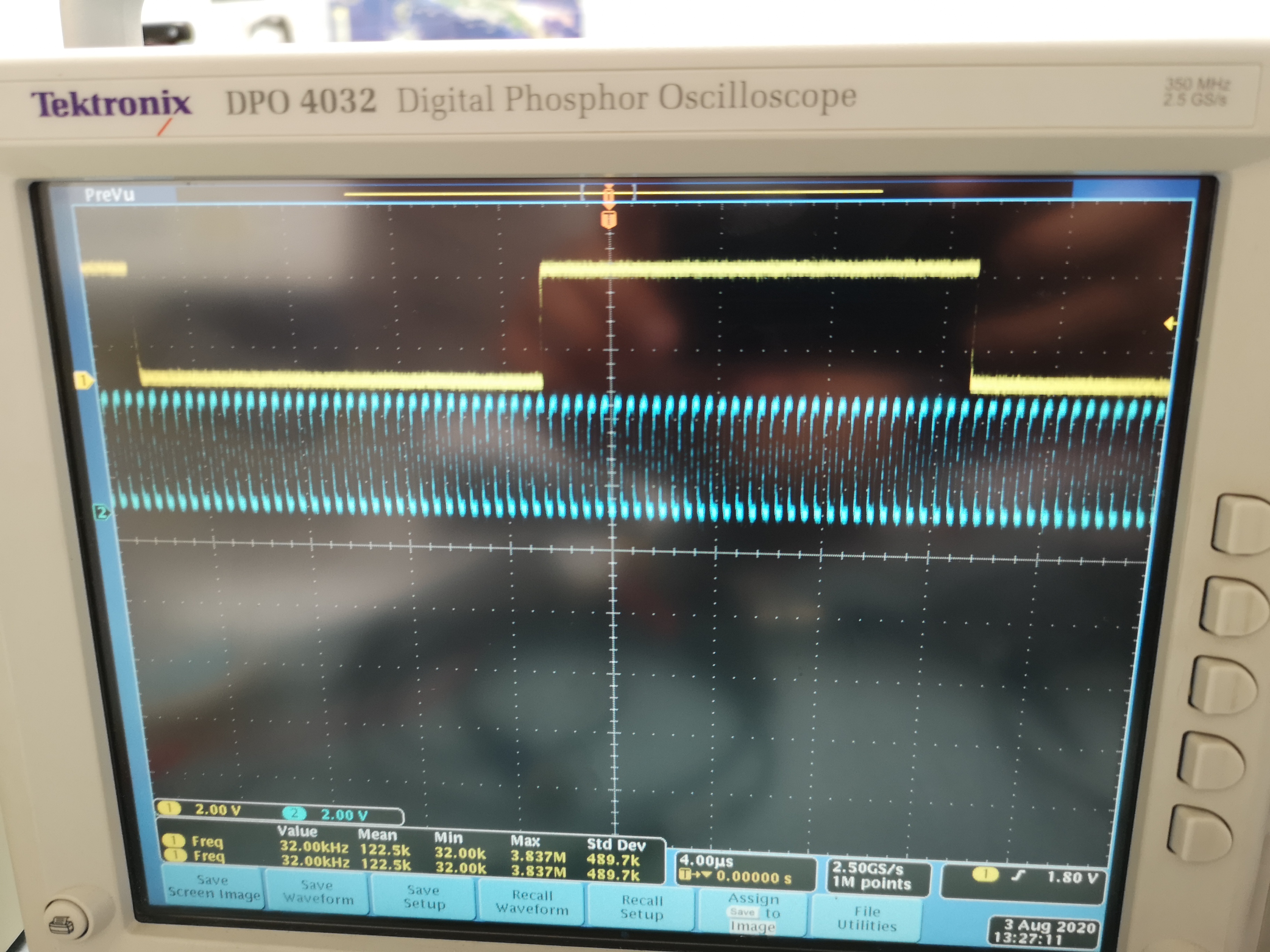
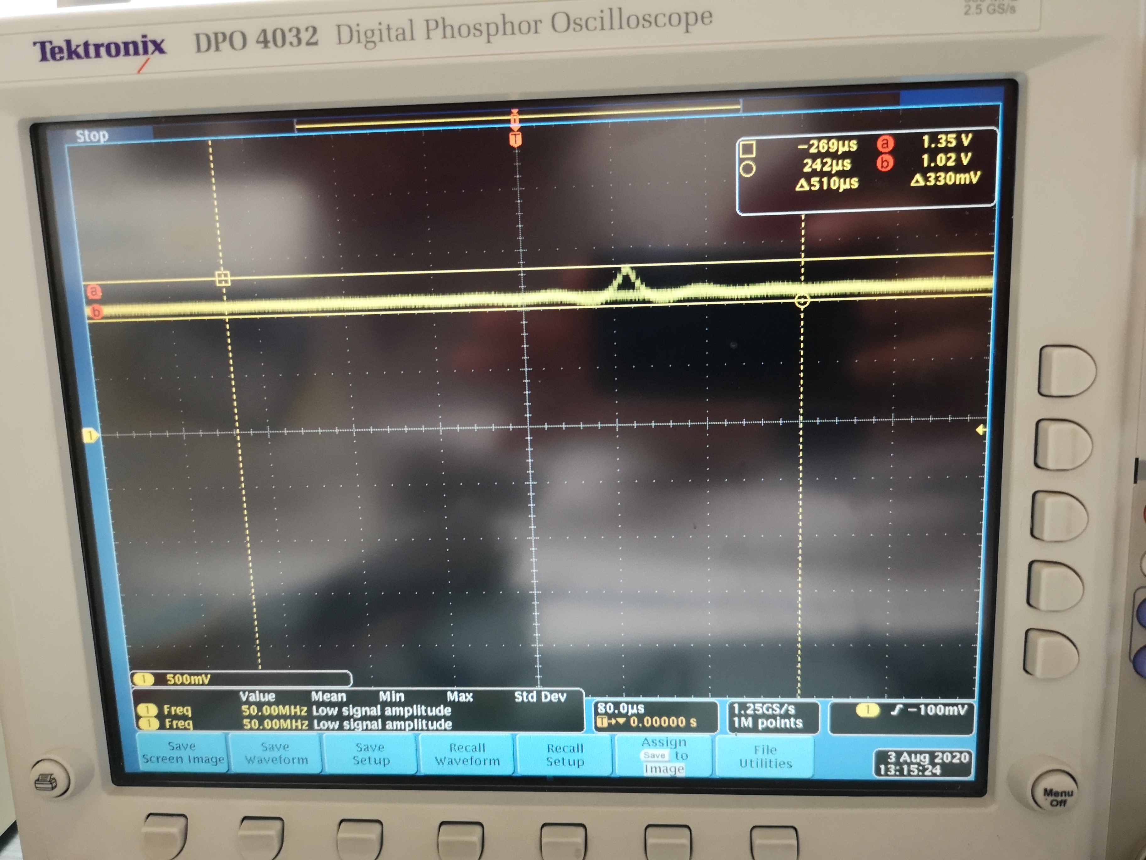
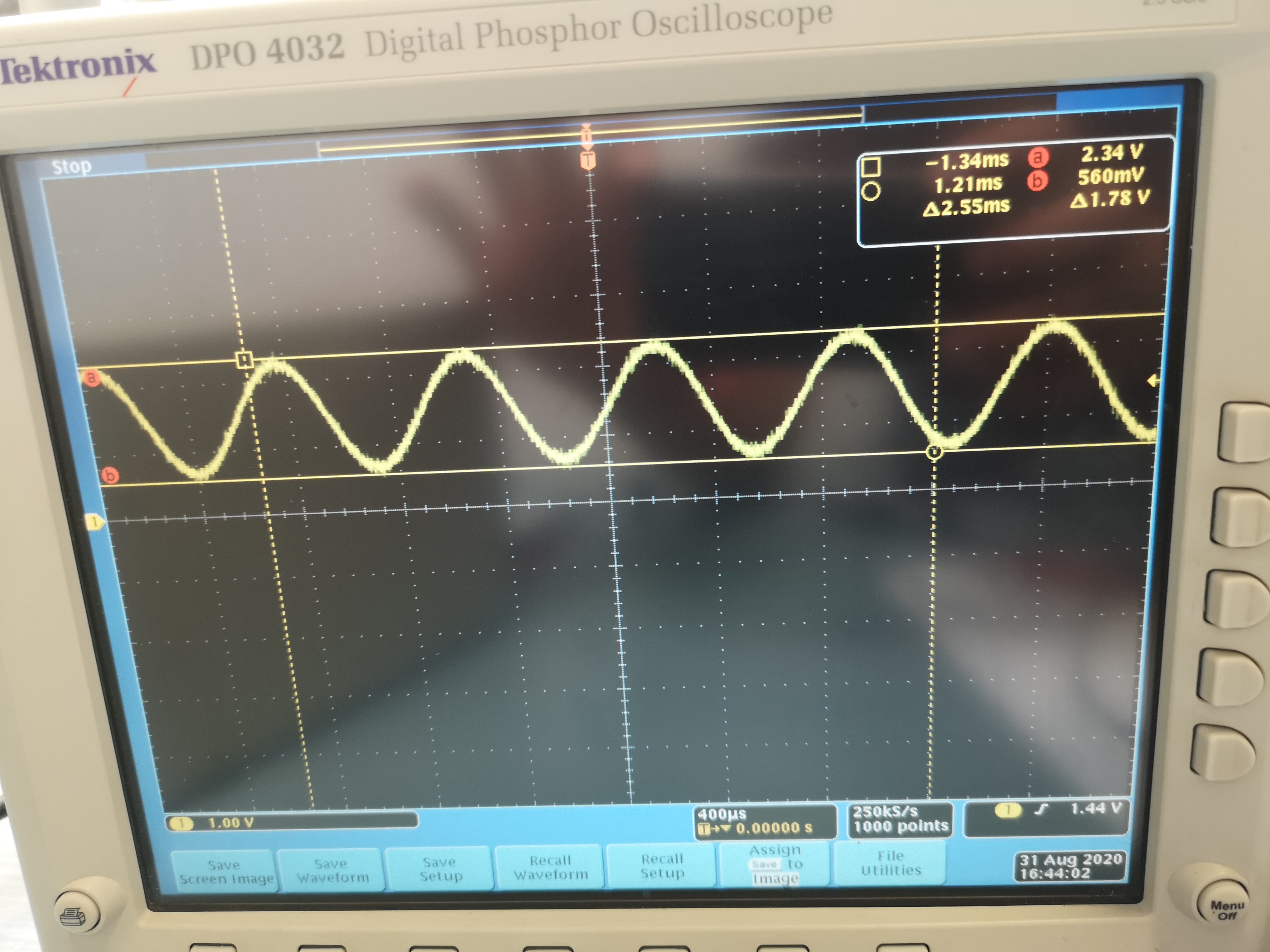
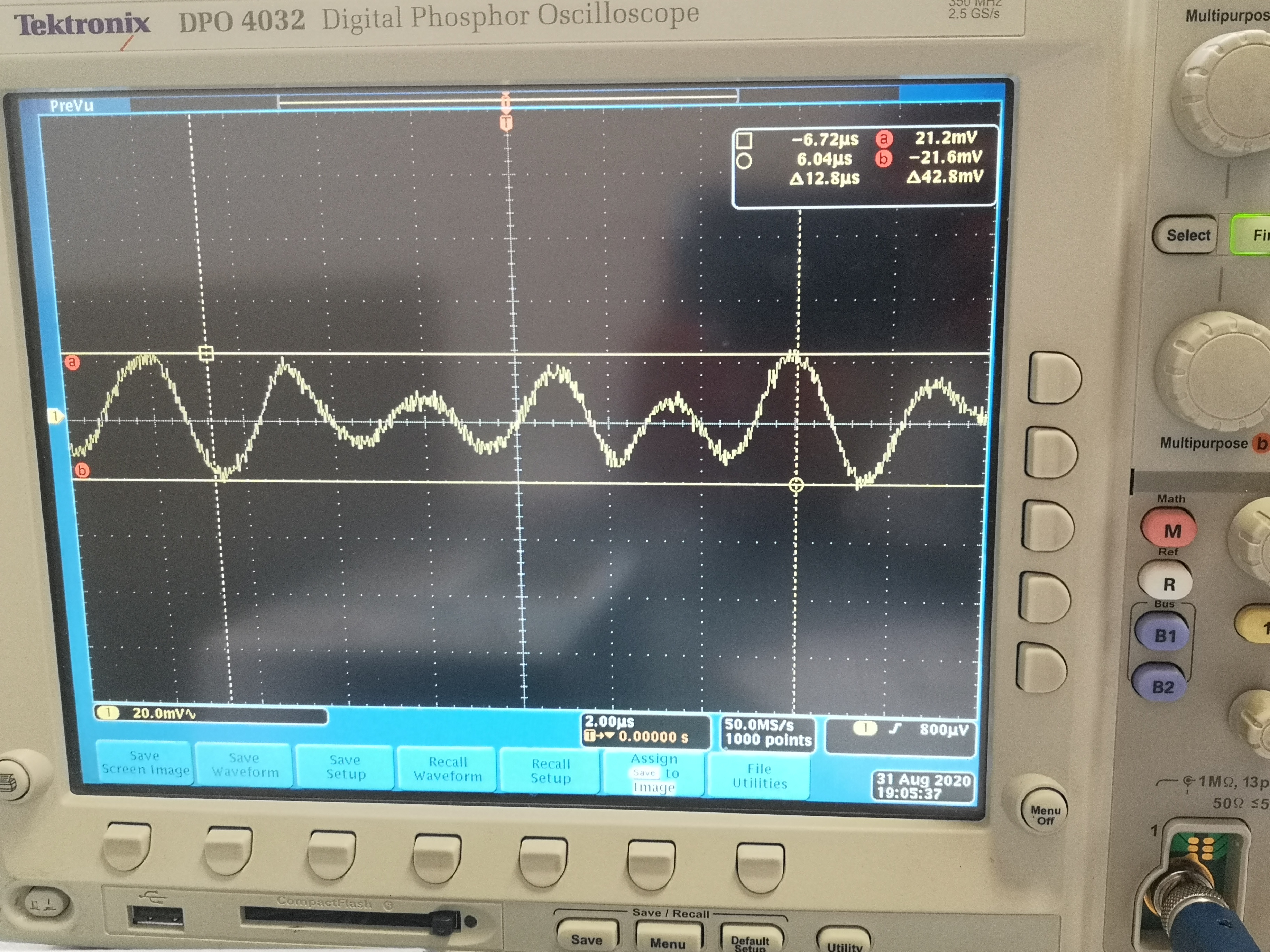
Hi, I need a DAC with AES/EBU input, so I used DIR9001 and PCM1793. The problem is that left signal from PCM1793 is not correct (is not a sine) . Could you please check the schematic below? Thanks in advance.

  • Hi Claudio,

    If the LEFT output is not a sine wave, what is it? Could you share an scope output of the channel compared to RIGHT output?

    Thanks,

    Paul

  • Does the digital source have a sine wave driven on the left channel?

  • Hi Paul,

    thank you for responding back. Anyway, I made some corrections on the schematic:

    The problem now is that left and right signals are different.

    This is the left:

    This is the right:

  • Hi Andy,

    as I've responded to Paul, I've modified the circuit and the problem is that left and right channels are different. The generator works correctly, indeed I used it with an other DAC.

  • Hi Claudio,

    This looks similar to a formating issue of the I2S.  Is it possible your edge timing is marginal so that the DAC is latching the data offset by 1 bit?  A good check would be to just invert the LRCK and see if the issue switches to the right channel.  I recommend you capture a few I2S frames to see if the data is in the correct bit position.

    Thanks,

    Paul

  • Hi Paul,

    I've inverted the LRCK and the issue switches to the right channel, so it concerns the same two pins. Anyway, I've captured a I2S frame and the data is in the correct position(as you can see in the image),so I don't know how I can solve this problem.

  • Hi Claudio,

    My concern is that your LRCK seems to be at 1.8V logic but the BCK is 3.3V  Could this be an MCU issue?  The minimum VIH (voltage-input: high) level for this device is 2V.  Seems like you are on the border of that so you could be seeing inconsistent results. Try correcting that first.

    Thanks,

    Paul

  • Hi Paul,

    in that image there wasn't the LRCK, but the DATA, anyway I've controlled all the DAC input signals and they respect the datasheet voltage values(as you can see in the images), so maybe the problem is the DAC and I should substitute it.

    LRCK

    DATA and BCK:


    SCK:

  • Can you measure the PCM output on the pins themselves? I think you should compare VOUTL+, VOUTL-, VOUTR+, VOUTR- to check if the error is actually being created in the output amplifier stage.

    Thanks,

    Paul

  • Hi Paul, I've just send you the images from the PCM output, I've disconnected the output stage because the issue starts from PCM.

    these are VOUTL+ and VOUTL-:

    These are VOUTR+ and VOUTR-:

    Thanks,

    Claudio

  • This is very interesting.  I think we are at the point where we must confirm the actual data on the bus.  Now I am pretty confident the DIR and PCM are configured correctly (both 24-bit standard I2S).  

    Can you set you SPDIF input to be a square wave at fS/2? As the output seems to have some kind of rectification, I am concerned the MSB of the DIN line is being incorrectly sampled or ignored.

  • Can you show LRCLK and the data on the same trace? And then LRCLK and BCLK?

    Is LRCLK truly 64 bit clocks wide, with 32 for left and 32 for right?

    If you had a four-channel 'scope you could monitor BCLK, LRCLK and data at the same time, that would help.

  • Hi Paul,
    I set the AES-EBU input to generate a square wave at f=32 Khz(fS=48 Khz,but my generator can't sample below 32 Khz and accepts loaded signals only with fs = 48 Khz),  so this is VOUTL-/VOUTL+:

    and this is VOUTR-/VOUTR+:

  • Hi Andy,

    these are LRCLK and DATA:

    and these are LRCK and BCK:

    so it seems correct.

  • Have you been able to change your digital source? For example, use a different source for the DIR9001.  I would like to rule out the digital source being an issue.  I would be worthwhile to verify if the data is actually correct.  A square wave would make that easier.

  • The VOUTR trace looks like what happens when you feed the DAC an impulse (delta function) -- one sample at full scale with all other samples zero. You can see the sinc from the reconstruction filter. (BTW, you should have a sinc function sample/wave file for testing DACs.)

    So that is a clue.

    I can't count how many BCLKs you have in LRCLK high and low time.

    Maybe the DAC chip is bad? I'm not a fan of shotgunning parts. Do you have another board built up that you can test?

  • Yes Paul, as I wrote you yesterday I used a square wave at fs=32 Khz, I post again the results:

    VOUTL-/VOUTL+:

    VOUTR-/VOUTR+:

    Moreover, I've tried all the other sources available in my generator(sweep, chirp, delay,pnoise,wnoise,polarity,dolby,dts) and the right output wave on the dac is always cutted, so I think that it is damaged. Anyway, before mounting another one, is the schematic correct in your opinion? My major doubt is about the connection between the AES/EBU input and DIR9001.

  • There are 32 BCLKs in LRCK high and 32  in low time, I've also checked the analogical and the digital feed of the dac and they are correct, so I think that the dac chip is damaged and I've ordered other 2 chips.

  • Hi Claudio,

    Sorry for the confusion, when I saw that square wave I thought it was the LRCK, not the output.  This looks as expected, where two channels are not latching the MSB correctly.

    I think at this point replacing the device is the best option.  

    The AES input looks okay to me, but I am not 100% on your source.  I do not think that would cause this issue.

    Thanks,

    Paul

  • Ok Paul,

    I'll replace it and I'll keep you updated.

    Thank you,

    Claudio

  • Hi Paul,

    I've finally replaced PCM1793, so now VOUTL-/VOUTL+ and VOUTR-/VOUTR+ are correct:

    The problem now is on the left/right signals:

    so I think I did some mistakes in the final stage.

    How can I modify the circuit?

    Regards,

    Claudio

  • Can you confirm some DC measurements around the final stage? Could the output be clipping? Is there any assembly issues?  You are also zoomed in quite a bit.  Can you widen the time scale to the same 400µs/division?  You might be seeing the actual switching of the delta-sigma modulator.

  • Hi Paul,

    I've finally solved the problem: I forgot to put the bypass capacitor between the ground and the inverting input of LM833.

    Best regards,

    Claudio Fiorentini