Because of the Thanksgiving holiday in the U.S., TI E2E™ design support forum responses may be delayed from November 25 through December 2. Thank you for your patience.

This thread has been locked.

If you have a related question, please click the "Ask a related question" button in the top right corner. The newly created question will be automatically linked to this question.

PCM3168A: Not passing FCC: Recommendations to reduce EMI

Part Number: PCM3168A

Hello,

We are building a consumer product using two PCM3168A parts and are having trouble passing FCC testing.

Our design is in a small metal enclosure and uses two PCM3168A's. We have isolated the noise and believe it is coming from the audio section, including the codec. A previous design with a competitor's part passed FCC. So, we think the circuit surrounding the PCM3168A is the issue. It is below.

We added L16 on the second pass at the suggestion of our factory. It didn't seem to make much difference. MCLK, SCLK, FCLK, and MOSI have 100 Ohm series resistors in another drawing close to the MCU.

We're using both codecs in slave mode, single rate clocking, with an MCLK of 12.288 MHz.

Do you have any recommendations on how to reduce the noise? Are we missing anything?

Thank you very much.

Aaron Higgins

  • Hi Aaron,

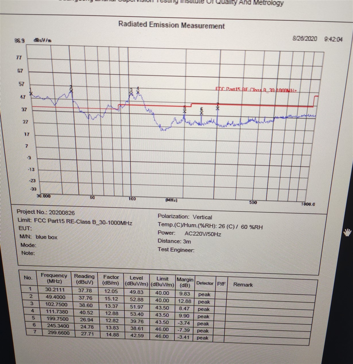
    Could you share a plot of the emissions spectrum so we could take a look at the results?  Are the spurs at multiples of the MCLK frequency? Do you have any series impedance on these lines near the driver to help reduce edge rates and ringing?

  • Yes, the MCLK and related lines have 100 Ohm series impedance. We also tried a ferrite bead on those lines, without much effect.

    Following is the plot:

  • Thank you for sharing.  What is your MCLK frequency and if you stop sending clocks do the results improve dramatically?

  • Thanks for the response. 

    MCLK is 12.288MHz. I believe this is the lowest available frequency when using the ADC (at 48kHz). Is there another we should try?

    I'm dealing with a remote and offsite lab and don't have an easy way to try what you suggest.

    Can you recommend some reasonable test equipment? I bought an RF Explorer for $400, but it doesn't seem to provide any meaningful data. I'm happy to try some experiments--I just want to be able to do them locally. 

    Our test engineer did attempt to isolate the problem by disconnecting the audio inputs and outputs. He also tried added a ferrite bead to the external audio wiring with good results.

    I appreciate any other thoughts you have to offer. Thank you.

    Aaron

  • Hey Aaron,

    To Collin's point, the clock and data lines are the only switched nodes for the device that are likely to contribute much to EMI. The 100 Ohm resistance you have generally helps a lot with this so it is good that you have them! If you have the ability to disable the clocks that would be a good way to check if this is the source of the issue. Alternatively, you could try running MCLK at 384*fs (18.432MHz) to see if this shifts the emission spurs. 

    We don't generally do this testing internally at the moment so I hesitate to make any equipment recommendations.

    How are you powering the codecs? Do you use any switched mode power supplies in your circuit? These, along with microprocessors, are very common sources of EMI. Unfortunately outside of the series resistance and ferrite beads that you have used, a lot of EMI suppression boils down to layout. There are many sources out there for best practices for layout but here are some of the common recommendations:

    • Make sure you have a solid ground plane and that all of the traces on your board (particularly the switched ones) have low inductance paths back to the ground plane. Multi-layer boards generally make this a lot easier to achieve, but sometimes you have to be weary of via inductance as well and it helps to have multiple vias to reduce this, especially on high current carrying traces.
    • Avoid splitting ground planes unless you absolutely need to. More often than not I tend to see split ground planes cause more issues than they resolve. If your a bit restricted in layout and need to split the planes to avoid digital noise coupling into the analog path that is understandable, but this must be done carefully because split planes effectively create slot antennas that can act as excellent radiators! If you do split the planes, make sure to connect them at a single point very close to the IC. 
    • From your schematic it looks like you have sufficient bypass capacitance around PCM3168A, so maybe just make sure this is the case for other components in the design too.

    Best,

    Zak

  • We are using switched power supplies in our design. It's powered from USB so one of the challenges is generating a split supply for the analog as well as a clean +5VA supply for the codecs.

    I'm starting to suspect the switching supply for the +5VA on the codec. One thing that now looks wrong is that the switching supply uses AGND for ground. That could be noisy. It could also use some more filtering.

    We do have separate digital and analog ground planes. I can confirm the single connection point is very close to the codec. Is there a better option here for analog and digital isolation? I have seen a single GND plane with a cutout used as a separator between analog and digital (see example below). Is this what you recommend?

    Thank you all,

    Aaron

  • Hi Aaron,

    I think the SMPS is the most likely culprit here. I have seen some devices provide an AGND for things like the feedback signal and any mode settings and a PGND for the main current path. It's also not uncommon to use a ferrite bead between your supply referenced to one ground and the bypass capacitance referenced to another. This creates an LC filter for high frequencies and a short for low frequencies. Here's an app note that discusses this in the context of PLLs, but it still applies https://www.ti.com/lit/an/scaa048/scaa048.pdf.

    I have never tried a cutout as a means of analog/digital isolation but I wouldn't recommend it because this means your current has to travel around this to return to ground, which means longer ground loops and more potential to radiate as a slot antenna. 

    Also you are probably aware but just remember that standard USB 2.0 protocol will only source up to 500mA of current without an external power source. This is increased for USB3.0 and USB-C, but if you are designing for compatibility with USB 2.0 the PCM3168A alone requires around 260mA between the analog and digital rails when all channels are active!

    Best,

    Zak