This thread has been locked.

If you have a related question, please click the "Ask a related question" button in the top right corner. The newly created question will be automatically linked to this question.

TPA3113D2: TPA3113D2 device and speaker damage

Part Number: TPA3113D2
Other Parts Discussed in Thread: TPA3110D2

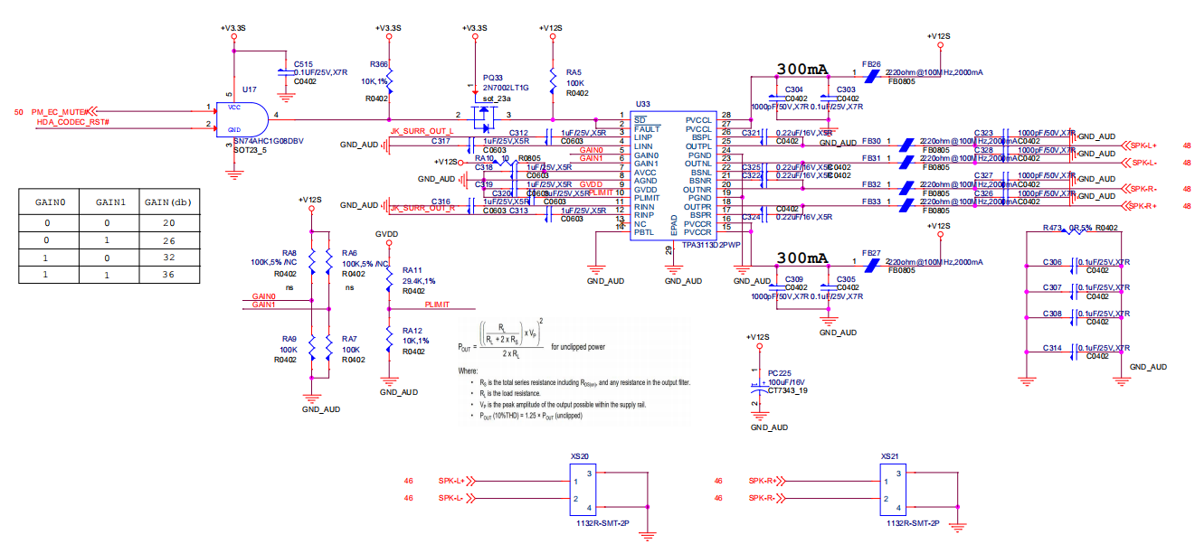
Hi, Would you help me to check the TPA3113D2 schematic?Speaker rated power is 8Ω1W. We have occurred some problem:

1,Does larger power output damage the speakers,the internal protect circuit adapt to the speaker loads to avoid damage?

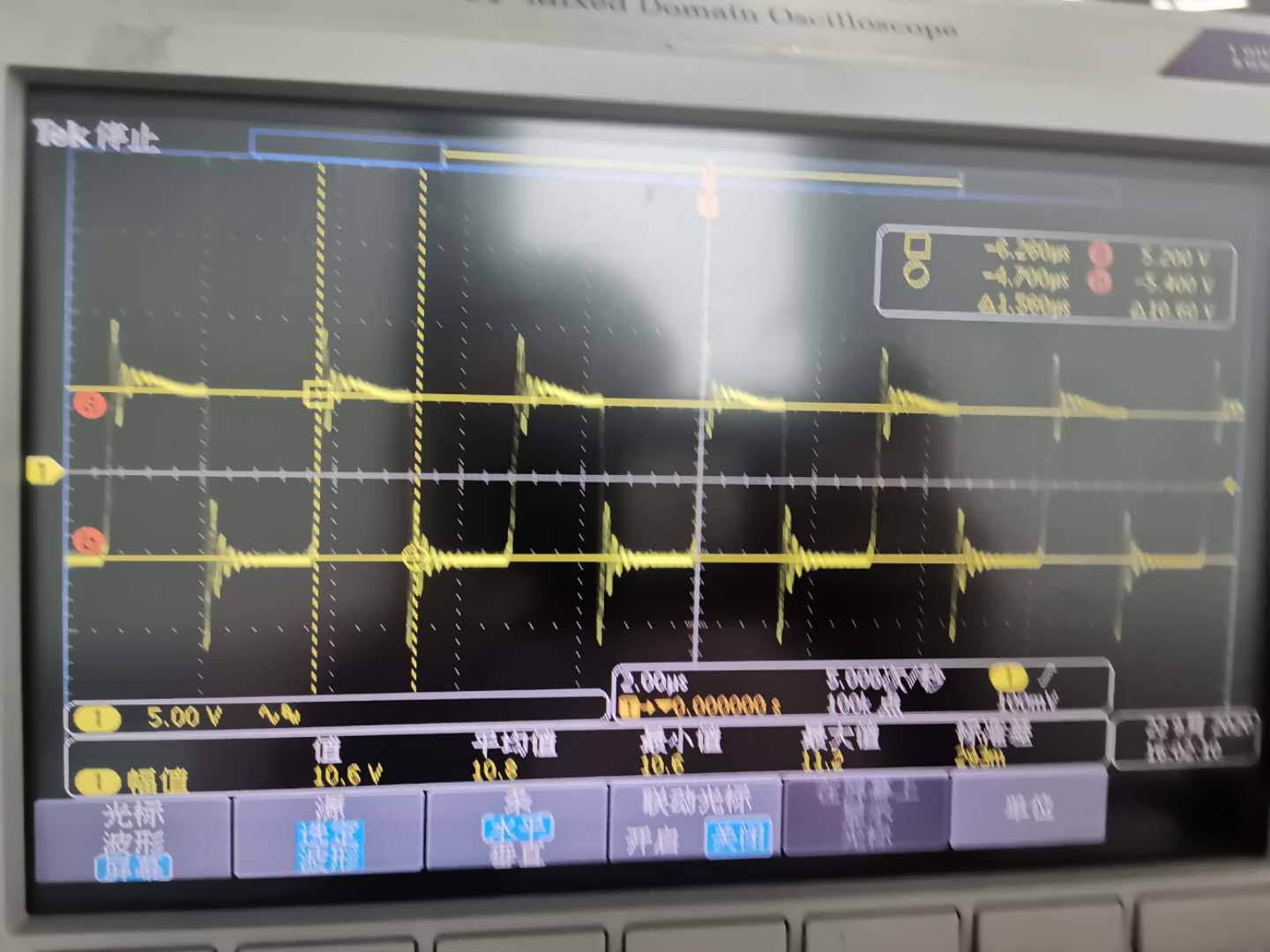
2,Some boards have no sounds output when powered on with the speakers load.Measure the pin1 /SD, transient voltage is 11V and then becomes 2V,the pin10 Plimit voltage is 7V.But removes the speakers when power on,the pin1 voltage is 11V,and plug in the speakers ,the two channels output sounds.It seems OK. However,when I replaced TPA3113D2 with a new device ,the pin1 /SD is 11V and PA output sounds during power on sequence,Is the device have damaged?What occurred,is the capture or components has some wrong parameters?

3,How to calculate Pout max?,In chapter 7.3.3 PLIMIT,the equation result is for singer channel or two output channel? The Rds(on) is 400mΩor 2X400mΩ?Someone has answered the similar question,but I didn’t understand.The table numbers calculate result is not match the equation.

4,I want to set the single channel Pomax 1W unclipped to protect the speakers, what is the Pin10 Plimit voltage?Follow the diagram,the Plimit is about 0.5V,but follow the equation,the result voltage is about 1.13V.Tpa3110d2 has the same description.


  • Hi,

    Thanks for your clear description!

    1) From your schematic, the AMP ground is separated. We do not recommend to separated AMP ground, just one completely ground plane is fine.

    2) Device has overcurrent protection, when load current exceed the OC threshold, device output will be Hi-Z and fault pin will be pull-up to high.

    3) You connect SD and Fault pins together, so when fault happened, the Fault pin will pull-low SD pin to recover device. So I think fault must happen, it seems OC fault, you can monitor the output current. I suggest you also can check Isat of beads and inductor of speaker, maybe start current exceed Isat. 

    4) The calculation in datasheet is for unclipped output power. The Table 2 list some clipped output power. So if you need unclipped power, please use the calculation.

    5)  According to your application, the calculation should be:

    1W=((8/(8+2*0.4))*Vp)^2/2*8. Then Vp=4.4V. 

    So PLIMIT voltage should be 1.1V. 

    Regards,

    Derek

  • Dear Derek,

        Thank you for your answer.If the device has been overcurrent protection,

    I'm unclear why after seal a new  device,the speaker module runs ok,and what‘s the threshold value when

    trigged the OV protection.

         Follow the equation, the single channel Poutmax=1W when PLIMIT=1.1V, but the graph shows it's about 3W when PLIMIT=1V.

    and there is another files" TPA311x-PLimit.pdf " indicate how to caculate the Pomax,the result is different.

    Is there some specific condicion to use the equation,to caculate unclipped  power?

  • Hi,

    That is why I suggest you to check output current when issue happened. The OC threshold is 3.5A, some devices may have very small variation.

    The calculation on datasheet(P15) is for unclipped power, if you need to calculate unclipped power, you should use this calculation, but it does not consider the output trace loss. The graph on datasheet shows the output power capacity, not for unclipped power.

    Regards,

    Derek 

  • Thank you,

           It seems the device has some variation,because there is no load,sometimes the PIN1 /SD is still 2V.

    If  I want to guarantee the 8Ω 1W speaker against  damage, I should follow the equation unclipped power 1W ,or follow the graph  output power capacity on the datasheet?

    and how to  caculate the power capacity?

    Thanks a lot

  • Hi,

    You should follow the equation unclipped power 1W, not graph.

    In theory, POUT (10%THD) = 1.25 × POUT (unclipped).

    Usually, we only consider 1% and 10% THD power application.

    Regards,

    Derek

  • Hi Derek,follow your suggestion, I set the  Plimit 1.05V, to make Po =1W,in order to protect the speaker 

    Why the  PA device output  square signal while there is no signal input?in

    When the input is Sin signal Vp-p 184V, the output is  square and has ring?

    and the output Vp-p reached 10V,( Av=20 dB),why the Plimit level hasn't limit the voltage?

    Is the waveform right?

    It is may test gragh below:

                             No voice input,the speaker waveform.

             Sin signal input wavfform 

                 Sin signal output waveform

  • Hi,

    The output voltage delivered to the speaker by class d amp is actually the differential voltage across the speaker. In idle status(no audio input), the OUTP and OUTN are both switching at 50% duty cycle, setting up a 1/2PVDD on each of the speaker terminal.

    The power stage of the class d amp is quite similar to the switching power supply. It switches at the frequency of hundreds of kHz. The waveform on switching node is PWM signal between 0V and PVDD.

    Regards,

    Sam

  • Thank you. It's the test waveform below.

    Test condition:Input  Sin sigal,1V/1K,Plimit=1V. Yellow line is speaker P,Blue is speaker N,and  Red is P-N.

    P-N is the load voltage on speaker.

    Follow the equation Pomaxunnclipped=1W. Pls help me to check the result if it's right?

  • Hi 

    What's the test point? AMP pins or load point?

    What's about load? speaker or resistor?

    Because you use inductor-free design, the beads can not filter switching noise, so I suggest you need add inductor on load or add external filter to filter switching noise firstly. 

    Regards,

    Derek

  • The load is speaker,and the test point is  the speaker P/N pin.

    The TPA3113 datasheet reference design has no inductor ,my petition is how to guarantee the speaker against damage,

    how to set the Pomax=1W

  • Thanks,

    The loader is spealer,and the testpoint is the speaker two PINS P/N.

    The design is refer to the referce design,my petetion is how to set the Pomax=1W?

    It seems there is some difference between theory and test result.

  • The tolerance is related to the external divider resistors and internal resistors. It can not fix the max power exactly.