This thread has been locked.

If you have a related question, please click the "Ask a related question" button in the top right corner. The newly created question will be automatically linked to this question.

PCM5122: SPI configuration

Part Number: PCM5122


Hello,

I am  using the above mentioned DAC(PCM5122) in one of my project.

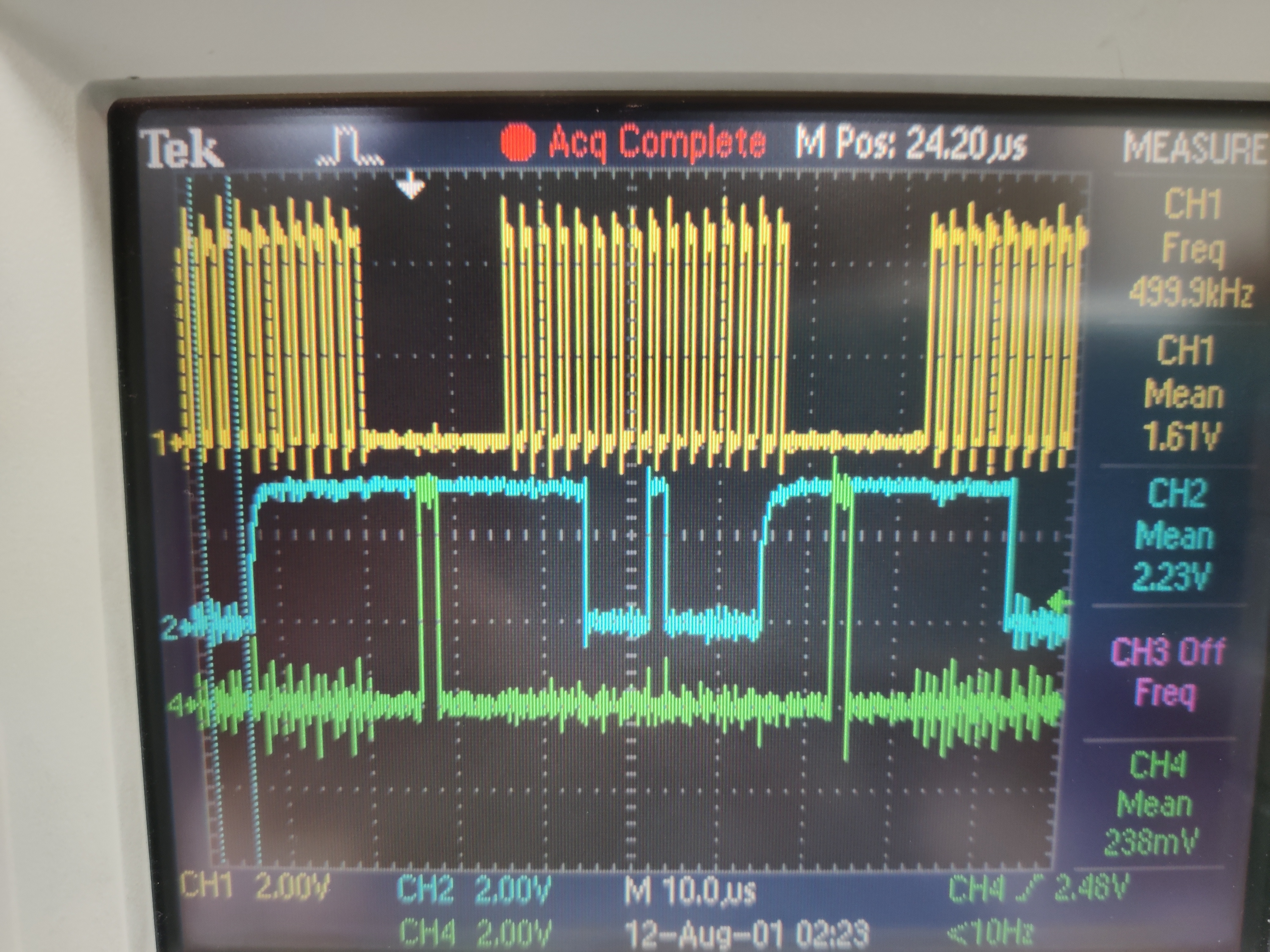
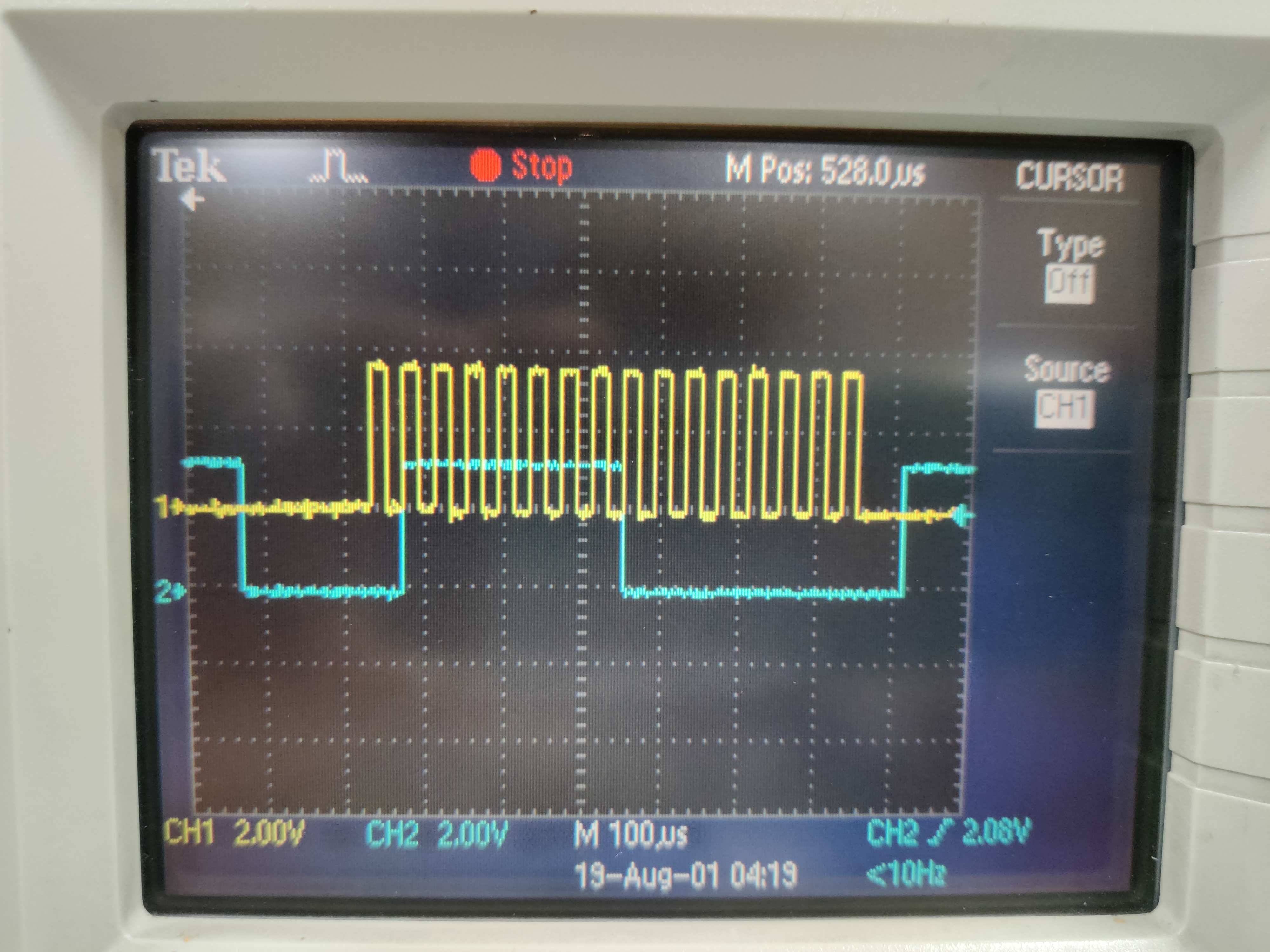
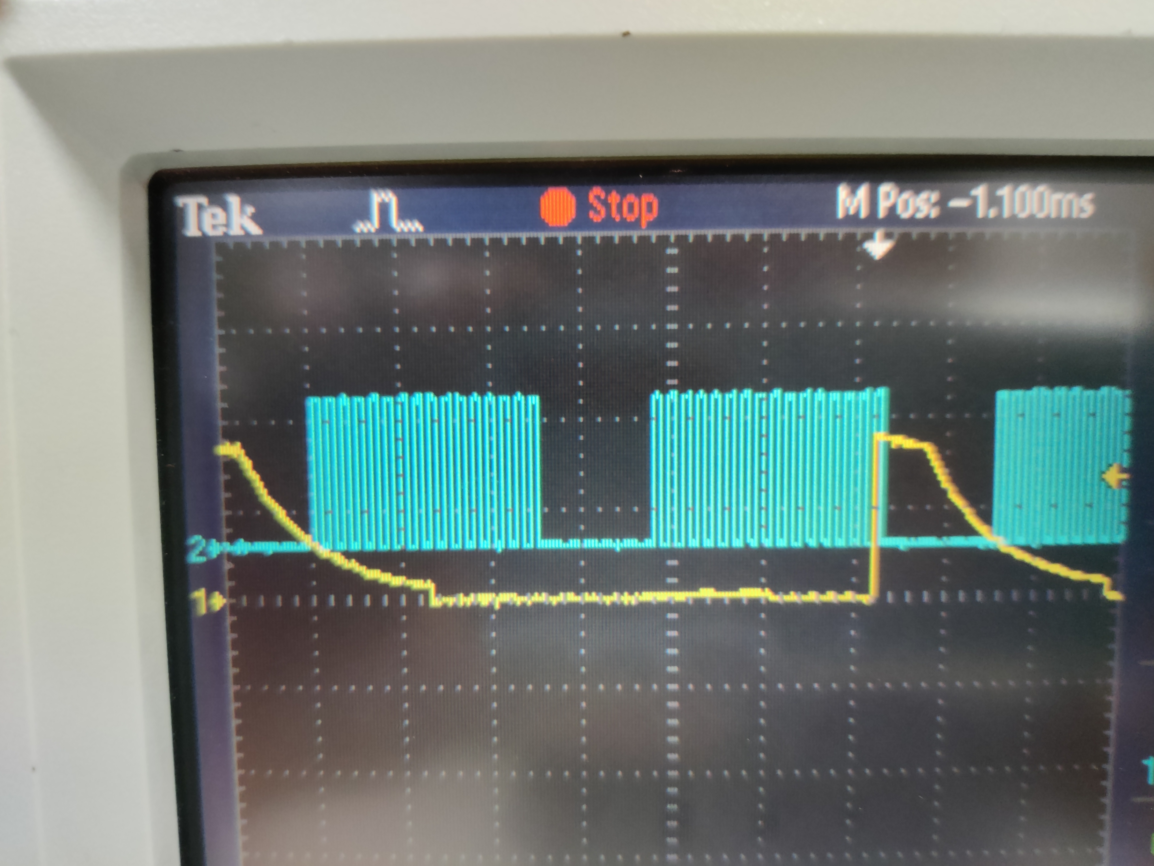
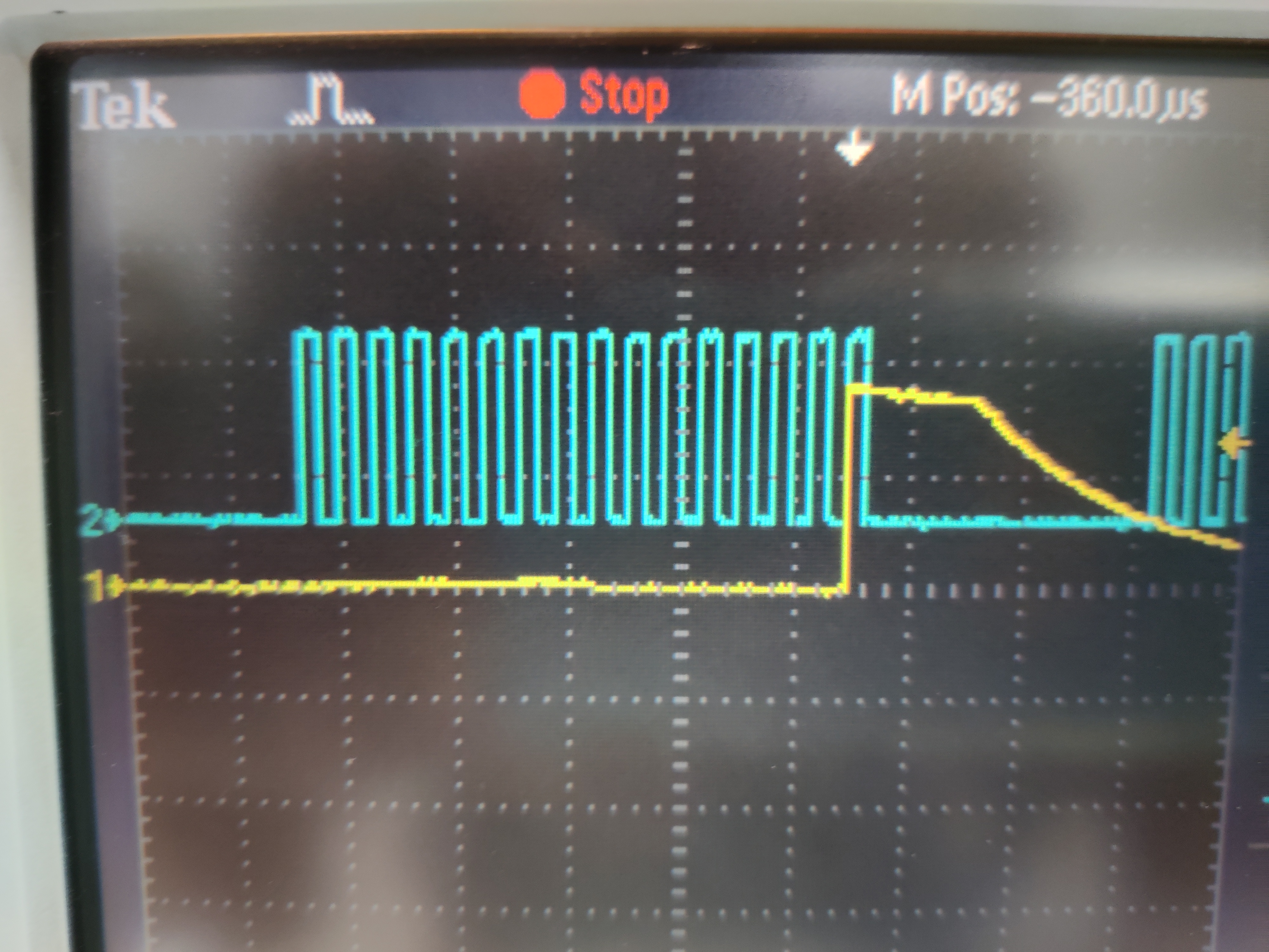
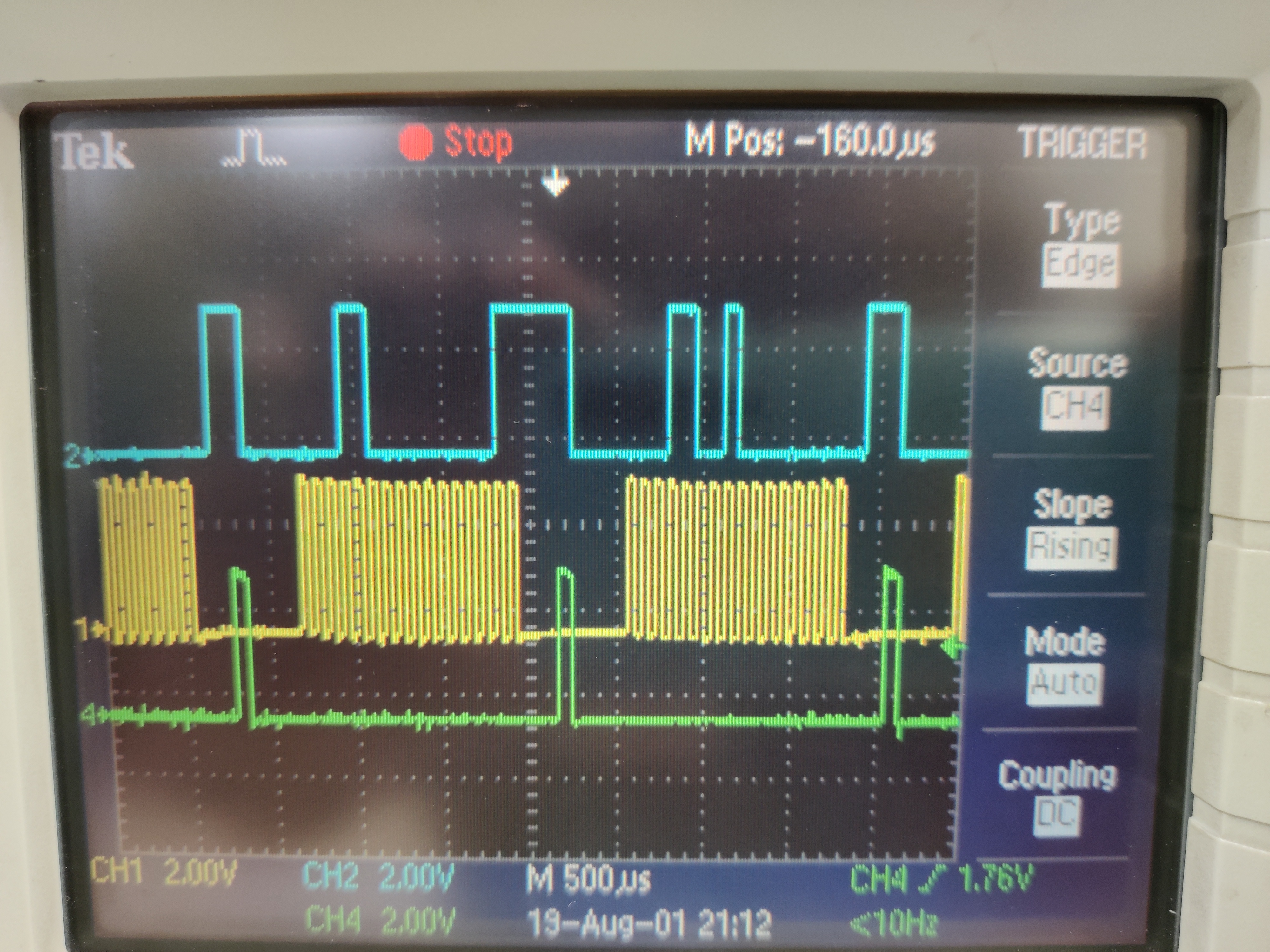
I am unable to perform  read/Write operations from/to the DAC using SPI configuration mode.

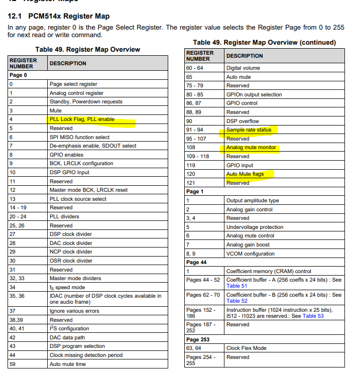
I would like to know  is there any specific sequence need to follow to access those registers and page selection. 

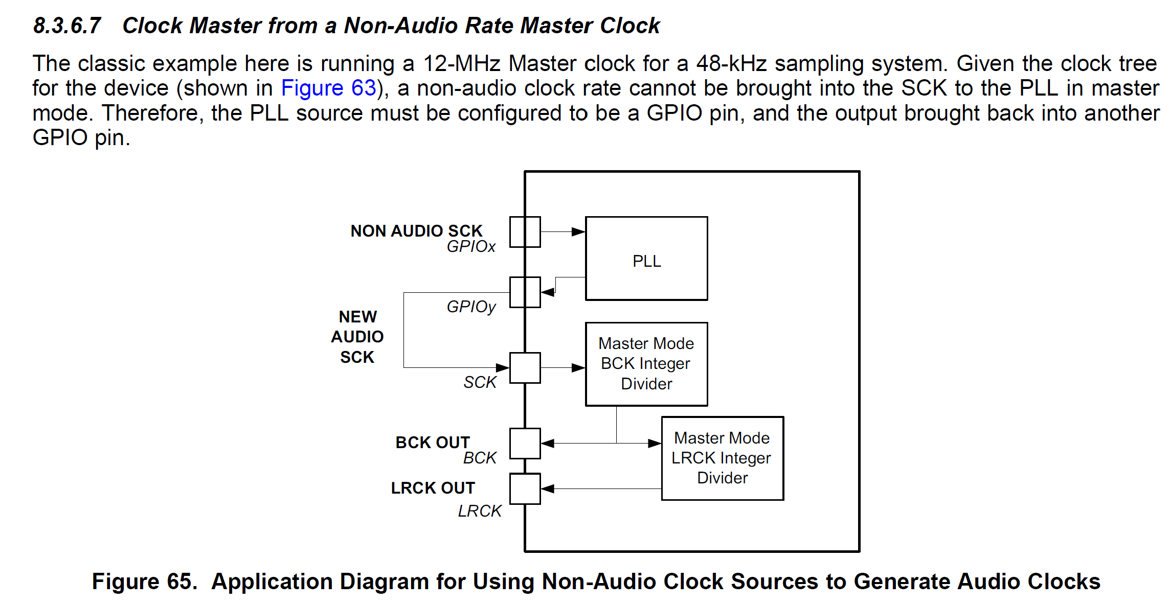
Please help me which registers I need to be configured for the master mode.  

Thanks and Regards

Sathish

  • Hi Sathish,

    Can you please share schematics of your circuit and Scope shots for your SPI frame?

    Regards,

    AK

  • Hi AK,

    Please go through the following attachments.

  • HI,

    Somehow the attachments you shared are missing from the post.

    Please attach using attach button in the e2e tool bar in edit mode.

    Do not copy and paste.

    Regards,

    AK

  • HI AK,

    Please  go through the attachments,

    Yellow referred to clock  MC of 500 khz,

    Green referred to chip select MS,

    Blue referred to data (MOSI) -- 7F00(to read register 63/page 0)

  • HI AK,

    Please  go through the attachments,

    Yellow referred to clock  MC of 500 khz,

    Green referred to chip select MS,

    Blue referred to data (MOSI) -- 7F00(to read register 63/page 0)

  • Hi,

    Your frames looks fine to me. Please make sure you are probing these on the PCM side.

    Can you show me what you got on SDO? is it still tri stated? if so first try to read status register and let me know what that is.

    Also in your schematics , I can see two separate ground connections, both are shorted somewhere on board? if not please do the same.

    Regards,

    AK

  • Hi AK,

    Yes, we are getting same frames at the PCM side also.

    Blue is referred to SDO(MISO) --> currently on the board I made it to pull up with 4.7k. and the data on the SDO pin is continuously toggling irrespective of register we are trying to read. I am  trying to read the page0 / register 63 which is having the default value of  0x2020.

    Yes, the two grounds are shorted.

    Regards

    Sathish

  • Hi AK,

    If the Device is in power down, can we do the SPI operations?

    And help us how to bring the device to normal mode if it is in power down mode?

    We are not getting any voltage at the VNEG pin is it causes anything ?

    Regards

    Sathish

  • Hi Sathish,

    Unless valid I2S data is received, device will not give anything on Charge pump out. Are you giving I2S signals to DAC after power up?

    When a clock error (SCK, BCK, and LRCK) or clock halt is detected, the PCM512x device automatically enters standby mode. The DAC and line driver are also powered down.When BCK and LRCK remain at a low level for more than 1 second, the PCM512x device automatically enters power down mode. Power-down mode disables the negative charge pump and bias/reference circuit, in addition to those disabled in standby mode.

    When expected audio clocks (SCK, BCK, LRCK) are applied to the PCM512x device, or if BCK and LRCK start correctly while SCK remains at ground level for 16 successive LRCK periods, the device starts its power up sequence automatically.So please ensure that these signals are applied after powering up the device and make sure charge pump outputs -3.3V.

    After that you start SPI transactions.  This is my understanding for this device. Apps engineer supporting this device on vacation, so please expect delay in response. But try the suggestions i mentioned.

    Regards,

    AK

  • Hi AK,

    Thanks for the response.

    We are giving SCK clock to the Device Continuously.

    We want it to be operate in Master Mode , So unless the device gives LRCK and BCK clocks we are not able  give the  I2S data to the Device.

    Will negative Charge pump Causes the problem in SPI read/Write Operations? I think it doesn't.?

    Still we are unable to perform the Read/Write operations. Please help us to solve this issue as early as possible as it urgent.

    If possible please provide the Application engineer contact details.

    Regards,

    Sathish 

  • Hi,

    Application engineer for this device is on vacation.

    Can you let me know whats the SCK frequency you are giving to device? Is this a non audio rate master clock such as 12Mhz?

    If so you need to make some changes as per datasheet page no 51. Otherwise please follow the guidelines given in datasheet page no 50

    Also you can go through the below e2e thread where user has asked the same question and solutions and programming examples given there.

    https://e2e.ti.com/support/audio/f/6/t/267830?tisearch=e2e-sitesearch&keymatch=pcm5122%20master#pi320995=2

    Regards,

    AK

  • Hi AK,

    Now I'm giving 12.288 MHz clock to the as SCK to the Device which is generating from the PLL in the FPGA.

    Will this SCK clock effects the SPI read/ Write operations? 

    To make the clock structure as fig_65 still I need to configure those registers through SPI interface which I am not able to do now.

    Thanks and Regards,

    Sathish

  • Hi Sathish,

    I am concerned that the command data/clock is being mis-latched due to some digital crosstalk.  I noticed in your screenshot, the SDO line seems to go high-z after 15 clock periods, not 16.  Can you significantly reduce your SPI CLK frequency as a quick test? Something like 10kHz should suffice. 

    Another good test would be to write a register and attempt to read it back.  Also not that SCK should be provided, which I believe you are now doing.

    Thanks,

    Paul

  • Hi Paul,

    SDO signal is not going to high after every 15 clock periods, continuously it is varying.

    I have tried with register write  and read back from that register but still I didn't get.

    I'm giving 12.288 MHz clock to the SCK it  may has tolerance, is it okay ? or do i need to give some other frequency?

  • The SCK for the I2S signal should be fine, I am more concerned about the SPI clock signal.  Can you reduce the communication speed of the SPI signal to see if that improves things?  Thanks,

    Paul

  • Hi Paul,

    We have given the 25 KHz of SPI clock still we are not getting anything on the SDO pin, we are trying to read the register 3F(63).

    I'm attaching the scope shots below please go through it.

    Thanks & Regards

    Sathish

  • Hi Paul,

    We have given the 12.5 KHz of SPI clock.

    We able to see the SDO is going to high at the 16th rising edge of the SPI clock for every read operation irrespective of the register we are trying to read, Scope shorts attached below.


    Thanks & Regards

  • Hi Vinay,

    This is very interesting behavior.  Is your CS line consistent? Could it be getting pulled high intermittently?  Many MCUs require you to monitor the SPI TX buffer before allowing CS to go high or it may assert high before the module is done sending the whole command.  It would be useful to monitor all three signals at the same time.  For example, in first image in the previous post, it seems like CS is staying low between the two 16-bit commands (as MISO does not enter Hi-Z).  

    Can you confirm:

    SCK is being provided?

    VNEG is ~-3V?

    LDOO is ~1.8V

  • Hi Paul,

    SCK is 12.288 MHz given.

    VNEG  it is coming around 500mv.

    LDO is coming 1.8V.

    We are trying the write  into the register 12 and reading from the same register

     Blue is referred MOSI and data is 0x1803(writing to 12 register) and 0X1900(reading from 12 register)

     Green is referred to MISO in the second image.


  • Hi Paul,

    Can you please help us by sharing the required register details to configure the DAC outputs.

    We are working in the MASTER MODE,SCK is 12.288 MHZ


    Thanks and Regards

    Sathish

  • Hi Sathish,

    You will need to do the following steps:

    #### CLK divider setting ###################
    #### Use VREF PLL settings when in VREF mode to look up the sample rate, and the SCK ## 
    #### In this example, look for 48kHz rate, with 12.288MHz SCK ####
    
    # Disable Auto Clock Configuration
    w  25 72
    # PLL P divider to 3
    w  14 03 
    # PLL J divider to 12.D1D2
    w  15 0C 
    # PLL D1 divider to J.00
    w  16 00 
    # PLL D2 divider to J.00
    w  17 00
    # PLL R divider to 1
    w  18 00
    # miniDSP CLK divider (NMAC) to 2
    w  1B 01
    # DAC CLK divider to 16
    w  1C 0F
    # NCP CLK divider to 4
    w  1D 03
    # OSC CLK divider is set to one (as its based on the output from the DAC CLK, which is already PLL/16)
    w  1E 00
    # FS setting should be set to single rate speed (48kHZ).
    w  22 00
    # IDAC1 sets the number of miniDSP instructions per clock. (set to 1024)
    w  23 04
    # IDAC2 
    w  24 00
    #############################################
    
    #### Master mode setting ####################
    # BCK, LRCK output
    w  09 11
    # Master mode BCK divider setting (making 64fs)
    w  20 03
    # Master mode LRCK divider setting (divide BCK by a further 64 to make 1fs)
    w  21 3F
    # Master mode BCK, LRCK divider reset release
    w  0C 7F
    ##############################################
    
    #### Stand-by request and release ############
    # Stand-by request
    w  02 10
    # Stand-by release
    w  02 00
    ##############################################

    Were you able to resolve the communication issues?

    Thanks,
    Paul

  • Hi Paul,

    Thanks for the response.

    Now we are able to perform the read and write operations on SPI Interface with 25 Khz as SPI clock.

    In the above mentioned registers, we are writing Master mode setting related registers and Stand-by request and release.

    As per the hardware the device is in VCOM mode, Do we need to  write the PLL configuration registers or not?

    Also we able to see the  -3.3 V at the VNEG pin, LRCK and BCK clock signals.

    We are trying to perform the I2S interface by writing 16 -bit data with respect to the LRCK and BCK.

    Status of the OUTL and OUTR is reaming at low irrespective of data.

    Please help us if we are missing any register.

    Thanks and Regards

    Sathish

  • You should verify that the I2S data is formatted correctly based on the FMT configuration you are using, i.e. I2S standard, RJ, LJ.  You should also confirm that the bit length matches what you have configured the PCM to be using.

    Otherwise, you should read the various status register to see if the device has any fault conditions, PLL lock issues, or "zero data detect" conditions.

    Thanks,

    Paul

  • Hi Paul ,

    Thanks for the response.

    I'll check the resepcted registers.

    I have selected the I2S INTERFACE with 16 bit data length.

    Please clarify below

    1.do we need to enable the PLL for this VCOM mode of operation.

    Can't we  get the output without enabling the PLL.?

    Regards

    Sathish

  • Hi Paul,

     I have checked the status registers,

    I have made the PLL Disable and observed the same.

    I have disable the auto mute channel register(Page 0/Register 65(0x41)) and disable the analog mute register(Pag1/Register6). But the Analog Mute channel register(Page0/register 108) is showing the channels are muted.

    Still OUTR and OUTL are remaining  at LOW.

    Thanks and regards

    Sathish


  • Hi Vinay,

    Please read and post the values in the status registers as well:

    It is possible the PLL is not locked, which will force the device into mute.

    Also, the PLL is required for your operation.

    Thanks,

    Paul

  • HI Paul,

    We have not enabled the PLL. We are giving SCK from the external, What is the use of enabling the PLL please clarify?

    We have checked the above specified registers,

    In the sample Rate status registers we are getting as SCK ratio error! and Mute control registers status are coming as expected.

    Please Clarify what may be the reason and how many clocks we need to provide per sample and per channel to DAC?

    In Detail: How many BCK clocks we need to give wrt to the LRCK per one sample for 16-bit data. 

    Regards

    Sathish

  • Hi Paul,

    We have read the all the status registers which you have mentioned above, We are getting the All registers status correctly as expected.

    We are giving the I2S input as 16-bit data from  0x0000 to 0XFFFF, we have tried with multiple combinations in that range. Still the outputs are  at LOW.

    How come we know that the I2S data is latching to the DAC, is there any register will gives this I2S data status?

    Regards

    Sathish

  • Hi Sathish,

    The PLL is required, as there are many internal clocks signals needed by the device, such as for the charge pump and the DSP processor.  This device will not work with the PLL disabled in your configuration.

    The commands I gave you will configure the PLL to provide all of the internal clocks, so it is important that those commands be implemented.

    The BCK should be providing either 64×fs or 32×fs clock for the I2S data to be sent from the MCU to the PCM.  You should capture a scope shot of the LRCK, BCK, and DATA and verify that the format is correct.  

    Thanks,

    Paul