This thread has been locked.

If you have a related question, please click the "Ask a related question" button in the top right corner. The newly created question will be automatically linked to this question.

TLV320AIC34: The WCLK and BCLK can not been seen when TLV320AIC34 works in master mode

Part Number: TLV320AIC34
Other Parts Discussed in Thread: TLV320AIC3106

Dear all,

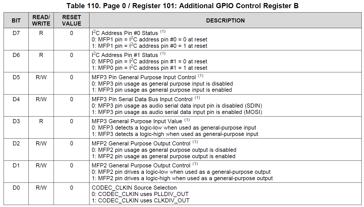
I designed a TLV320AIC34 board, and the TLV320AIC34 works in master mode. The GPIO2_A connects a external oscillator whose frequancy is 12.288MHz. I carefully ready TLV320AIC34's datasheet, especilly page 22. The CLKDIV_IN  is connected with GPIO2_A, CLKOUT_IN is connected with CLKDIV_IN, M is set to 1, N is set to 2. By this configuration, I can see a wave whose frequency equals to 12.288M via GPIO1_A.  The PLL_IN is connected to GPIO2_A,  R is set to 1, P is set to 1, J is set to 8, D is set 0,  the other configuration is default. Theoretically the sampling frequency is fs=(12.288e6*8*1)/(256*8*1)=48000 Hz. unfortunately, I can not see any signal from BCLK_A and BCLK_A. One more question, from Page 22, there is a switch denoted as CODEC_CLKIN, I can not find register that selects CLKDIV_OUT or PLLDIV_OUT.

The schematic and code are attached, can you help me to solve it. Thank you very much.TLV320AIC34.pdf 

  • Sorry! The code is here.

    uint8_t AIC34_Master_Slave_Set(uint8_t i2c_addr,uint8_t select, unsigned int fs)
    {
    
        if(select==MASTER)
        {
            uint8_t u_value=0;


            u_value=0;
            AIC34_ReadReg(i2c_addr,98,&u_value);
            u_value|=2<<4;             // GPIO1_x output = clock mux output divided by 1 (M = 1)
            u_value|=1<<3;             // GPIO1_x clock mux output = clock divider mux output
            AIC34_WriteReg(i2c_addr,98,u_value);
    
            u_value=0;
            AIC34_ReadReg(i2c_addr,102,&u_value);
            u_value|=1<<6;             // CLKDIV_IN uses GPIO2_x
            u_value|=1<<4;             // PLLCLK_IN uses GPIO2_x.
            u_value|=2<<0;             // N=2
            AIC34_WriteReg(i2c_addr,102,u_value);
    
    
            u_value=0;
            AIC34_ReadReg(i2c_addr,8,&u_value);
            u_value|=1<<7;             // BCLK_x (or GPIO2_x if programmed as BCLK_x) is an output (master mode).
            u_value|=1<<6;             // WCLK_x (or GPIO1_x if programmed as WCLK_x) is an output (master mode)
            u_value|=1<<5;             // 1: Place DOUT_x in high-impedance state when valid data is not being sent.
            u_value|=1<<4;             // BCLK_x (or GPIO2_x if programmed as BCLK_x) / WCLK_x (or GPIO1_x if programmed as
            // WCLK_x) continues to be transmitted when running in master mode, even if codec is powered down
            AIC34_WriteReg(i2c_addr,8,u_value);
    
    
            switch(fs)
            {
            case 48000:
                u_value=0;
                AIC34_ReadReg(i2c_addr,3,&u_value);
                u_value|=1<<0;                        //P=1
                AIC34_WriteReg(i2c_addr,3,u_value);
                u_value=0;
                AIC34_ReadReg(i2c_addr,3,&u_value);
    
                u_value=0;
                u_value|=0x08<<2;                      //J=8
                AIC34_WriteReg(i2c_addr,4,u_value);
    
                AIC34_WriteReg(i2c_addr,5,0);        //D=0
                AIC34_WriteReg(i2c_addr,6,0);
    
                u_value=0;
                AIC34_ReadReg(i2c_addr,11,&u_value);
                u_value|=1<<0;                        //P=1
                AIC34_WriteReg(i2c_addr,11,u_value);
    
    
                u_value=0;
                AIC34_ReadReg(i2c_addr,19,&u_value);
                u_value|=1<<2;
                AIC34_WriteReg(i2c_addr,19,u_value);
    
                u_value=0;
                AIC34_ReadReg(i2c_addr,22,&u_value);
                u_value|=1<<2;
                AIC34_WriteReg(i2c_addr,22,u_value);
                break;
            default:
                break;
            }
            AIC34_ReadReg(i2c_addr,3,&u_value);
            u_value|=1<<7;                        //PLL is enabled
            AIC34_WriteReg(i2c_addr,3,u_value);
        }
        return 1;
    }


  • Hello Yuehai,

    The configuration you explain seems to be correct. Just to make sure, can you please provide a register dump so I may look at all of the registers?

    The CODEC_CLKIN source is selected in register 101. There is a data sheet error and it is not shown. you may take a look at the TLV320AIC3106 data sheet for reference (The AIC34 is essentially 2 AIC3106's). I have also posted an image below.

    Regards,

    Aaron

  • Hi Aaron,

    Thank you for your help. I write down all the registers' value, and it is attached.  In the configuration, I break out the connection between external oscillator and GPIO2_A, and I connect external oscillator to MCLK_A, So in register 102, "CLKDIV_IN uses MCLK_A, and PLLCLK_IN uses MCLK_A" are selected. There is still no signal in BCLK_A and WCLK_A, from PIN_K3, PIN_K4, also there is no signal from DIN_A and DOUT_A. Can you help me please? Thank you very much.

    Best regards,

    Yuehai.

      0 -> 0x 0
      1 -> 0x 0
      2 -> 0x 0
      3 -> 0x91
      4 -> 0x20
      5 -> 0x 0
      6 -> 0x 0
      7 -> 0x 0
      8 -> 0xf0
      9 -> 0x 0
     10 -> 0x 0
     11 -> 0x 1
     12 -> 0x 0
     13 -> 0x 0
     14 -> 0x 0
     15 -> 0x80
     16 -> 0x80
     17 -> 0xff
     18 -> 0xff
     19 -> 0x7c
     20 -> 0x78
     21 -> 0x78
     22 -> 0x7c
     23 -> 0x78
     24 -> 0x78
     25 -> 0x 6
     26 -> 0x 0
     27 -> 0xfe
     28 -> 0x 0
     29 -> 0x 0
     30 -> 0xfe
     31 -> 0x 0
     32 -> 0x 0
     33 -> 0x 0
     34 -> 0x 0
     35 -> 0x 0
     36 -> 0xcc
     37 -> 0x 0
     38 -> 0x 0
     39 -> 0x 0
     40 -> 0x 0
     41 -> 0x 0
     42 -> 0x 0
     43 -> 0x80
     44 -> 0x80
     45 -> 0x 0
     46 -> 0x 0
     47 -> 0x 0
     48 -> 0x 0
     49 -> 0x 0
     50 -> 0x 0
     51 -> 0x 4
     52 -> 0x 0
     53 -> 0x 0
     54 -> 0x 0
     55 -> 0x 0
     56 -> 0x 0
     57 -> 0x 0
     58 -> 0x 4
     59 -> 0x 0
     60 -> 0x 0
     61 -> 0x 0
     62 -> 0x 0
     63 -> 0x 0
     64 -> 0x 0
     65 -> 0x 4
     66 -> 0x 0
     67 -> 0x 0
     68 -> 0x 0
     69 -> 0x 0
     70 -> 0x 0
     71 -> 0x 0
     72 -> 0x 4
     73 -> 0x 0
     74 -> 0x 0
     75 -> 0x 0
     76 -> 0x 0
     77 -> 0x 0
     78 -> 0x 0
     79 -> 0x 0
     80 -> 0x 0
     81 -> 0x 0
     82 -> 0x 0
     83 -> 0x 0
     84 -> 0x 0
     85 -> 0x 0
     86 -> 0x 0
     87 -> 0x 0
     88 -> 0x 0
     89 -> 0x 0
     90 -> 0x 0
     91 -> 0x 0
     92 -> 0x 0
     93 -> 0x 0
     94 -> 0x 0
     95 -> 0x 0
     96 -> 0x 0
     97 -> 0x 0
     98 -> 0x28
     99 -> 0x 0
    100 -> 0x 0
    101 -> 0x 0
    102 -> 0x 6
    103 -> 0x 0
    104 -> 0x 0
    105 -> 0x 0
    106 -> 0x 0
    107 -> 0x 0
    108 -> 0x 0
    109 -> 0x 0
    110 -> 0x 0
    111 -> 0x 0
    112 -> 0x 0
    113 -> 0x 0
    114 -> 0x 0
    115 -> 0x 0
    116 -> 0x 0
    117 -> 0x 0
    118 -> 0x 0
    

  • Hello Yuehai,

    Thanks for sharing this info. It looks like you are writing 0x06 to register 102. Is this correct? If so, this register is improperly getting configured. Bits D7-D4 should be 0101. This will select GPIO2 for CLKDIV_IN and PLLCLK_IN. 

    Please let me know if this works. 

    Regards,

    Aaron

  • Hi Aaron,

    Thank you! I tried to write 0x00 to register 102, it did not work. I found a bug in my schematic design, I connected AVDD_DAC to GND (PIN B3), but it should be connect to AVDD, so what will happen when AVDD_DAC connects to GND? It is the reason that the AIC34 does not work?

    Best regards,

    Yuehai.

  • Hello Yuehai,

    I am not exactly sure what might happen. Were you able to connect this to the proper supply level and check the fucntionality?

    Regards,

    Aaron

  • Hi Aaron,

    I am not able to connect to AVDD_DAC pin to proper supply level right now, I will design a new evaluation board later. Thank you for your help.

    Best regards,

    Yuehai.