


Part Number: TPA2008D2
Dear Teams,
Have a nice day and nice to meet you! Here is Dylan from China NWC MM team FAE. I am coming to approach you because I found there is a potential business growth opportunities for Class-D audio amplifier. I found you are also the owner of the TPA2008D2. Could I ask some support need from your team? If you are not the right person for technical support need, could you loop the correct person?
Support Need:
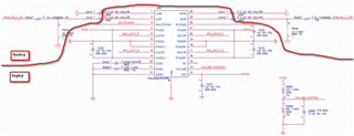
- Customer is confusing whether they should placed the PCB layout of TPA2008D2 with codec analog together for all, or the AMP input terminal should be placed into analog side? Or they should placed this chipset and speaker into digital side? Do you have any suggestions?
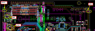
- In another case, due the position of speaker, there is no way to place AMP TPA2008D2 and speaker to the analog part of the Codec. Could you also give some suggestions?
Thanks!
Dylan
