


Other Parts Discussed in Thread: PCM1808, PCM1754, PCM1789, DIR9001, DIT4192, PCM1753
Tiny Tool Kits are reference designs for the fundamental devices of TI’s audio converter portfolio. These kits are low-cost development tools for the PCM1808, PCM1754, PCM1789, DIR9001, DIT4192 and a USB to I2C/I2S dongle. All of these board designs are very tiny and easy to use and evaluate. Below are basic guides to the 5 current TTK designs. Each guide has 8 parts:
- Part Description
- Board Description
- Inputs
- Outputs
- Control
- Basic Application
- More Information
- Schematic
The TTK designs can be built into one package to evaluate all of the devices: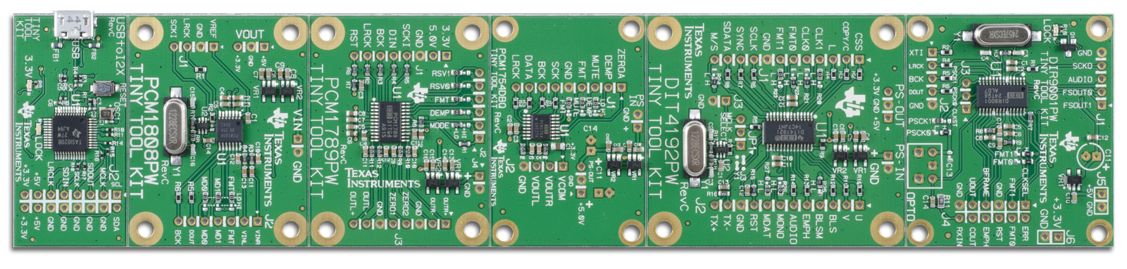
Four of the TTK designs can be connected together to create an audio system, for more information read:
3583.AudioSystem_TTK_Guide.docx
PCM1808 TTK Guide
Single-ended, Analog-input 24-bit, 96-kHz Stereo A/D Converter
1. Part Description
The PCM1808 is high-performance, low-cost, single-chip, stereo analog-to-digital converter with single-ended analog voltage input. The PCM1808 uses a delta-sigma modulator with 64-times oversampling and includes a digital decimation filter and high-pass filter that removes the dc component of the input signal. For various applications, the PCM1808 supports master and slave mode and two data formats in serial audio interface.
2. Board Description
The PCM1808 Tiny Tool Kit (TTK) contains the basic components necessary for converting single-ended analog audio into digital audio. In addition to the PCM1808 IC, the board has two voltage regulators (3.3V and 5V), a 12.288 MHz crystal and driver, as well as the necessary resistors and capacitors for operation (see schematic). Also on this board are junctions for header pins to test and evaluate the device.
3. Inputs
| Name | Junction | Pin # | Description |
| VIN | VIN | 1 | Input DC voltage (+5 to +24V) |
| GND | VIN | 2 | Ground |
| SCKI | J1 | 4 | Digital audio, system clock |
| VINR | J2 | 1 | Analog audio, right channel |
| VINL | J2 | 2 | Analog audio, left channel |
4. Outputs
| Name | Junction | Pin # | Description |
| VREF | J1 | 1 | Voltage reference |
| LRCK | J1 | 4 | Digital audio, left/right (frame) clock |
| DOUT | J2 | 6 | Digital audio signal |
| BCK | J2 | 7 | Digital audio, bit clock |
| +5V | VOUT | 1 | +5V DC output from LDO |
| GND | VOUT J1 | 2 2 | Ground |
| +3.3V | VOUT | 3 | +3.3V DC output from LDO |
5. Control
| Name | Junction | Pin # | Preset | Description |
| FMT | J2 | 3 | Low | Audio interface format select |
| MD1 | J2 | 4 | Low | Audio interface mode select 1 |
| MD0 | J2 | 5 | Low | Audio interface mode select 0 |
| R2 | 1-2 | When connecting 1-2, the PCM1808 uses an external system clock, provided through the CKI pin; when connecting 2-3, the PCM1808 uses the onboard 12.288 MHz crystal oscillator. |
WARNING: The FMT, MD1, or MD0 pins are all shorted to ground. The surface mount jumper must be removed before changing the setting on these control pins.
6. Basic Application
The PCM1808 TTK is setup to be in slave mode with an I2S 24-bit output and a 256x, 384x, 512x system clock auto detect. Converting single-ended analog audio into digital audio can be done in 3 steps:
- Connect single-ended analog audio input and system clock into the board
- Connect the I2S digital audio into the appropriate device for the application
- Power the device using a power supply or other DC source
For additional functionality, the control settings can be changed for different applications. One example is the R2 resistor can be modified to position 2-3. This changes the system clock input of the PCM1808 from using an external clock to the onboard 12.288MHz crystal. For a full list of control settings look at the PCM1808 datasheet.
7. More information
To get more information about the PCM1808 please look at the datasheet (PCM1808).
8. Schematic
1134.TTK-PCM1808PW_RevC-Schematic.pdf
PCM1754 TTK Guide
24-Bit, 192-kHz Sampling, Enhanced Multi-Level ΔΣ, Stereo, Audio Digital-to-Analog Converter
1. Part Description
The PCM1753/54/55 is a CMOS, monolithic, integrated circuit, which includes stereo digital-to-analog converters and support circuitry in a small 16-lead SSOP package. The data converters use TI’s enhanced multilevel delta-sigma architecture, which employs 4th-order noise shaping and 8-level amplitude quantization to achieve excellent dynamic performance and improved tolerance to clock jitter. The PCM1753/54/55 accepts industry standard audio data formats with 16- to 24-bit data, providing easy interfacing to audio DSP and decoder chips. Sampling rates up to 200 kHz are supported. A full set of user-programmable functions is accessible through a three-wire serial control port, which supports register write functions.
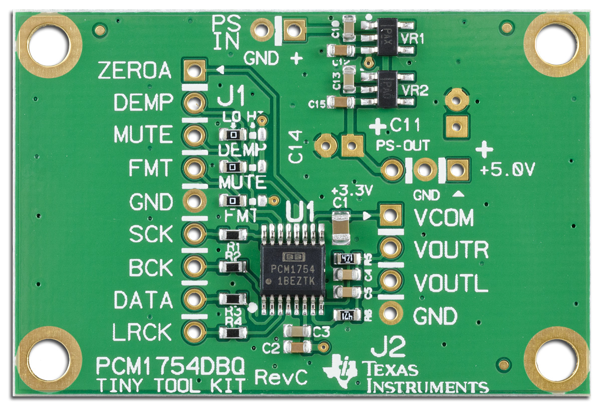
2. Board Description
The PCM1754 Tiny Tool Kit (TTK) contains the basic components necessary for converting digital audio into analog audio. In addition to the PCM1754 IC, the board has two voltage regulators (3.3V and 5V) as well as the necessary resistors and capacitors for operation (see schematic). Also on this board are junctions for header pins to test and evaluate the device.
3. Inputs
| Name | Junction | Pin # | Description |
| + | PS-IN | 1 | Input DC voltage (+5 to +24V) |
| GND | PS-IN | 2 | Ground |
| SCK | J1 | 6 | Digital audio, system clock |
| BCK | J1 | 7 | Digital audio, bit clock |
| DATA | J1 | 8 | Digital audio signal |
| LRCK | J1 | 9 | Digital audio, left/right (frame) clock |
4. Outputs
| Name | Junction | Pin # | Description |
| ZEROA | J1 | 1 | Zero flag output for L/R channels |
| VCOM | J2 | 1 | Common voltage decoupling |
| VOUTL | J2 | 2 | Analog audio, left channel |
| VOUTR | J2 | 3 | Analog audio, right channel |
| +5V | PS-OUT | 1 | +5V DC output from LDO |
| GND | PS-OUT J1 J2 | 2 5 4 | Ground |
| +3.3V | PS-OUT | 3 | +3.3V DC output from LDO |
5. Control
| Name | Junction | Pin # | Preset | Description |
| DEMP | J1 | 2 | Low | De-emphasis control |
| MUTE | J1 | 3 | Low | Analog mixing control |
| FMT | J1 | 4 | Low | Data format select |
WARNING: The DEMP, MUTE, and FMT pins are shorted to ground. The surface mount jumper must be removed before changing the setting on these control pins.
6. Basic Application
The PCM1754 TTK is setup with a 16-24 bit I2S signal as the output with de-emphasis off. Converting digital audio to analog audio can be done in 3 steps:
- Connect I2S digital audio input into the board
- Connect the output analog audio into an amplifier
- Power the device using a power supply or other DC source
For additional functionality, the control settings can be changed for different applications. One example is the MUTE pin can be used to mute the output. However, this requires removing the onboard jumper. For a full list of control settings look at the PCM1754 datasheet. Furthermore, the ZEROA pin can be used to verify that there is a non-zero analog audio signal at the left and right channel outputs.
7. More information
To get more information about the PCM1754 please look at the datasheet (PCM1754).
8. Schematic
6607.TTK-PCM1754DBQ_RevC-Schematic.pdf
PCM1789 TTK Guide
24-Bit, 192-kHz Sampling, Enhanced Multi-Level ΔΣ, Stereo, Audio Digital-to-Analog Converter
1. Part Description
The PCM1789 is a high-performance, single-chip, 24-bit, stereo, audio digital-to-analog converter (DAC) with differential outputs. The two-channel, 24-bit DAC employs an enhanced multi-level, delta-sigma (ΔΣ) modulator, and supports 8 kHz to 192 kHz sampling rates and a 16-/20-/24-/32-bit width digital audio input word on the audio interface. The audio interface of PCM1789 supports a 24-bit, DSP format in addition to I2S, left-justified, and right-justified formats.
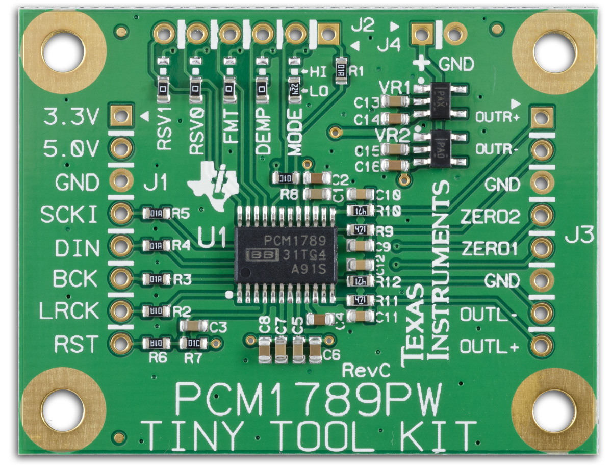
2. Board Description
The PCM1789 Tiny Tool Kit (TTK) contains the basic components for converting digital audio into differential analog audio. In addition to the PCM1789 IC, the board has two voltage regulators (3.3V and 5V) as well as the necessary resistors and capacitors for operation (see schematic). Also on this board are junctions for header pins to test and evaluate the device.
3. Inputs
| Name | Junction | Pin # | Description |
| + | J4 | 1 | Input DC voltage (+5 to +24V) |
| GND | J4 | 2 | Ground |
| SCKI | J1 | 4 | Digital audio, system clock |
| DIN | J1 | 5 | Digital audio signal |
| BCK | J1 | 6 | Digital audio, bit clock |
| LRCK | J1 | 7 | Digital audio, left/right (frame) clock |
4. Outputs
| Name | Junction | Pin # | Description |
| OUTR+ | J3 | 1 | Analog audio, positive right channel |
| OUTR- | J3 | 2 | Analog audio, negative right channel |
| ZERO2 | J3 | 4 | Zero detect flag output 1 |
| ZERO1 | J3 | 5 | Zero detect flag output 2 |
| OUTL- | J3 | 7 | Analog audio, negative left channel |
| OUTL+ | J3 | 8 | Analog audio, positive left channel |
| 3.3V | J1 | 1 | +3.3V DC output from LDO |
| 5V | J1 | 2 | +5V DC output from LDO |
| GND | J1 J3 | 3 3,6 | Ground |
5. Control
| Name | Junction | Pin # | Preset | Description |
| RST | J1 | 8 | High | Reset and power-down, active low |
| AMUTE1 | J2 | 1 | High | Analog mute control, active low |
| MODE | J2 | 2 | Low | Control port mode selection |
| DEMP | J2 | 3 | Low | De-emphasis control (H/W mode) |
| FMT | J2 | 4 | Low | Format select (H/W mode) |
| RSV0 | J2 | 5 | Low | Reserved (H/W mode) |
| RSV1 | J2 | 6 | Low | Reserved (H/W mode) |
WARNING: The MODE, DEMP, FMT, RSV0, and RSV1 pins are shorted to ground. The surface mount jumper must be removed before changing the setting on these control pins.
6. Basic Application
The PCM1789 TTK is setup in hardware mode with a 16/20/24/32 bit I2S input signal with de-emphasis off. Converting digital audio to analog audio can be done in 3 steps:
- Connect I2S digital audio input into the board
- Connect the output audio into an amplifier
- Power the device using a power supply or other DC source
For additional functionality, the control pins can be used to mute the output as well as reset and power-down the device. In order to mute or power-down the device, the appropriate pin must be grounded. For a full list of control settings look at the PCM1789 datasheet. Furthermore, the ZERO1 and ZERO2 pins can be used to verify that there is a non-zero analog audio signal at the left and right channel outputs.
7. More information
To get more information about the PCM1789 please look at the datasheet (PCM1789).
8. Schematic
4382.TTK-PCM1789PW_RevC-Schematic.pdf
DIR9001 TTK Guide
96-kHz, 24-Bit Digital Audio Interface Receiver
1. Part Description
The DIR9001 is a digital audio interface receiver that can receive a 28-kHz to 108-kHz sampling-frequency, 24-bit-data-word, biphase-encoded signal. The DIR9001 complies with IEC60958-3, JEITA CPR-1205 (Revised version of EIAJ CP-1201), AES3, EBUtech3250, and it can be used in various applications that require a digital audio interface. The DIR9001 supports many output system clock and output data formats and can be used flexibly in many application systems. As the all functions which the DIR9001 provides can be controlled directly through control pins, it can be used easily in an application system that does not have a microcontroller. Also, as dedicated pins are provided for the channel-status bit and user-data bit, processing of their information can be easily accomplished by connecting with a microcontroller, DSP, etc.
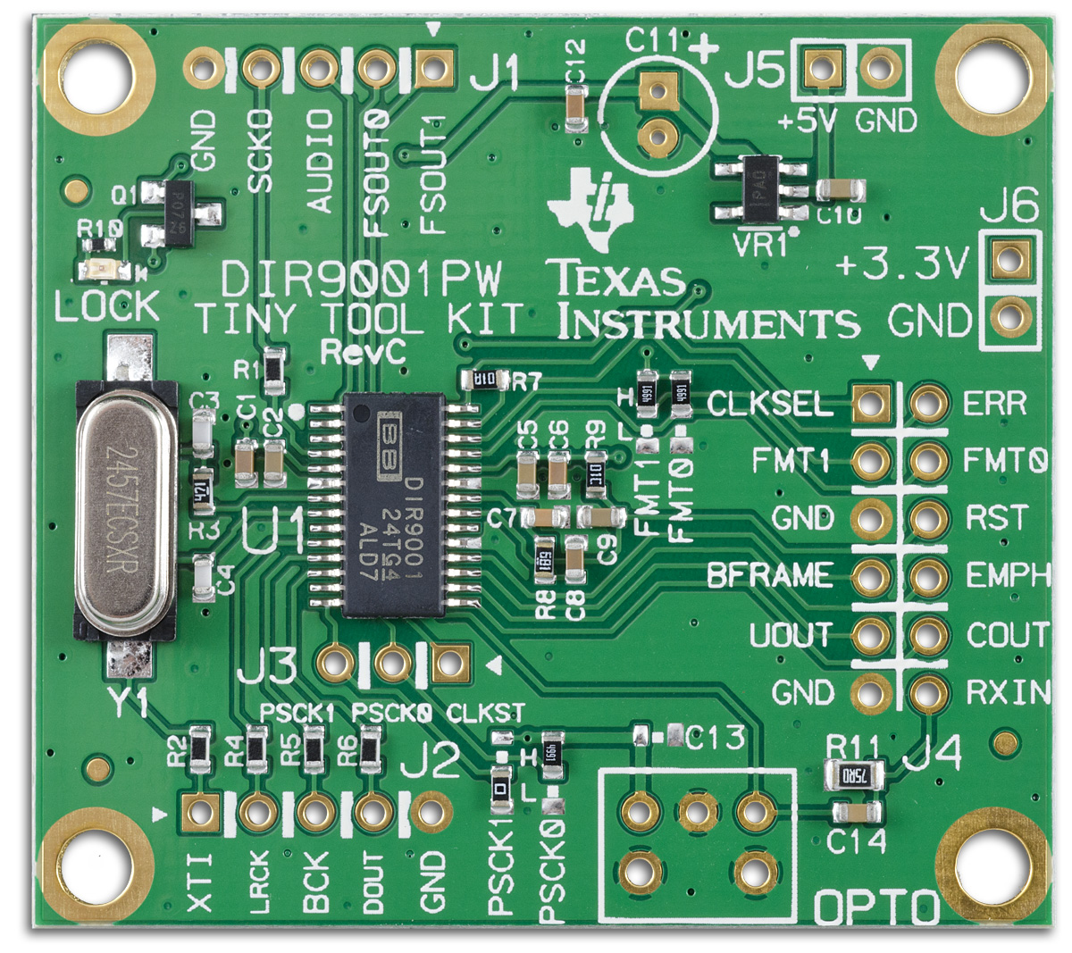
2. Board Description
The DIR9001 Tiny Tool Kit (TTK) contains the basic components necessary for receiving digital audio interface signals. In addition to the DIR9001 IC, the board has a junction for an optical receiver, a 24.576MHz crystal, and the necessary resistors and capacitors for operation (see schematic). There is an indicator LED on this TTK to indicate a lock on the interface audio signal. Also on this board are junctions for header pins to test and evaluate the device.
3. Inputs
| Name | Junction | Pin # | Description |
| +5V | J5 | 1 | Input DC voltage, +5V |
| GND | J5 | 2 | Ground |
| RXIN | J6 | 2 | Digital audio interface receive signal |
NOTE: The audio input for the DIR9001 TTK can also come through the optic port, if installed.
4. Outputs
| Name | Junction | Pin # | Description |
| FSOUT1 | J1 | 1 | Actual sampling frequency calculated result 0 |
| FSOUT0 | J1 | 2 | Actual sampling frequency calculated result 1 |
| AUDIO | J1 | 3 | Channel-status data information of non-audio sample word, active low |
| SCKO | J1 | 4 | Digital audio, system clock |
| LRCKO | J2 | 2 | Digital audio signal |
| BCKO | J2 | 3 | Digital audio, bit clock |
| DOUT | J2 | 4 | Digital audio, left/right (frame) clock |
| CLKST | J3 | 1 | Clock change/transition signal |
| ERROR | J4 | 2 | Indication of internal PLL or data parity error |
| BFRAME | J4 | 7 | Indication of top block of biphase input signal |
| EMPH | J4 | 8 | Channel-status data information of pre-emphasis |
| UOUT | J4 | 9 | User data serial output synchronized with LRCKO |
| COUT | J4 | 10 | Channel-status data serial output synchronized with LRCKO |
| +3.3V | J6 | 4 | +3.3V DC output from LDO |
5. Control
| Name | Junction | Pin # | Preset | Description |
| PSCK0 | J3 | 2 | Low | PLL source SCKO output frequency selection 0 |
| PSCK1 | J3 | 3 | High | PLL source SCKO output frequency selection 1 |
| CKSEL | J4 | 1 | NC | Selection of system clock source |
| FMT1 | J4 | 3 | High | Decoded serial digital audio data output format selection 1 |
| FMT0 | J4 | 4 | High | Decoded serial digital audio data output format selection 0 |
| RST | J4 | 6 | High | Reset control input, active low |
WARNING: The PSCK0 pin is shorted to ground. The surface mount jumper must be removed before changing the setting on this control pin.
6. Basic Application
The DIR9001PW TTK is setup for hardware control with a 24-bit I2S digital output and a system clock rate (SCKO) of 256 Fs. Converting a digital audio interface signal to an I2S digital audio signal can be done in 3 steps:
- Connect the digital audio interface input into the board
- Connect the I2S digital audio into the appropriate device for the application
- Power the device using a power supply or other DC source
For additional functionality, the control pins can be used to reset as well as change the system clock output frequency and the digital audio format. For a full list of control settings look at the DIR9001 datasheet.
7. More information
To get more information about the DIR9001 please look at the datasheet (DIR9001).
8. Schematic
2620.TTK-DIR9001PW_RevC-Schematic.pdf
DIT4192 TTK Guide
192kHz Digital Audio Transmitter
1. Part Description
The DIT4192 is a digital audio transmitter designed for use in both professional and consumer audio applications. Transmit data rates up to 192kHz are supported. The DIT4192 supports both software and hardware operation, which makes it suitable for applications with or without a microcontroller. A flexible serial audio interface is provided, supporting standard audio data formats and easy interfacing to audio DSP serial ports.
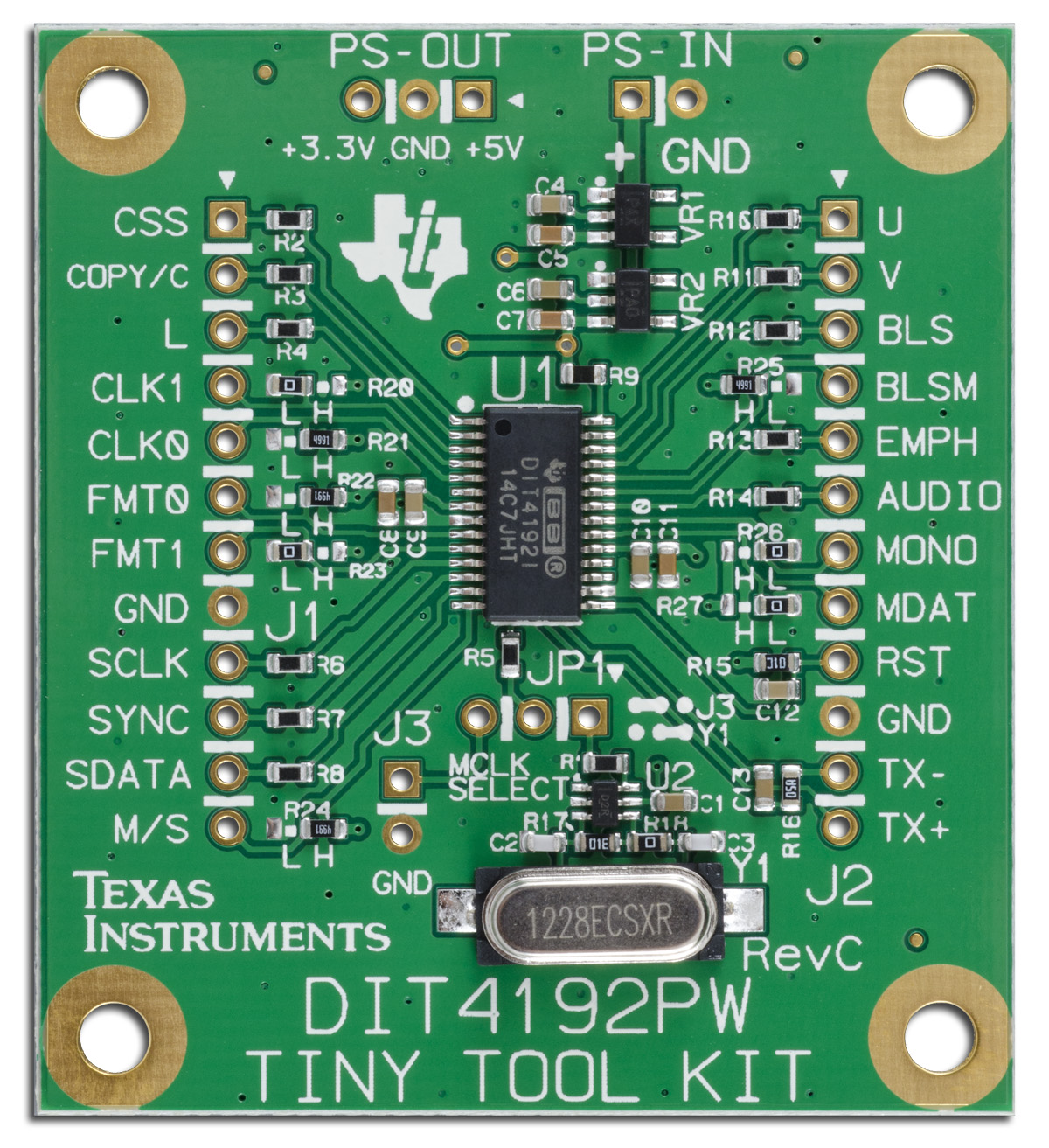
2. Board Description
The DIT4192 Tiny Tool Kit (TTK) contains the basic components necessary for transmitting digital audio. In addition to the DIT4192 IC, the board has two voltage regulators (3.3V and 5V), a 12.288MHz crystal and driver, as well as the necessary resistors and capacitors for operation (see schematic). Also on this board are junctions for header pins to test and evaluate the device.
3. Inputs
| Name | Junction | Pin # | Description |
| + | PS-IN | 1 | Input DC voltage (+5 to +24V) |
| GND | PS-IN | 2 | Ground |
| SCKI | J1 | 4 | Digital audio, system clock |
| DIN | J1 | 5 | Digital audio signal |
| BCK | J1 | 6 | Digital audio, bit clock |
| LRCK | J1 | 7 | Digital audio, left/right (frame) clock |
4. Outputs
| Name | Junction | Pin # | Description |
| TX- | J2 | 11 | Transmit negative |
| TX+ | J2 | 12 | Transmit positive |
| +5V | PS-OUT | 1 | +5V DC output from LDO |
| GND | PS-OUT | 2 | Ground |
| +3.3V | PS-OUT | 3 | +3.3V DC output from LDO |
5. Control
| Name | Junction | Pin # | Preset | Description |
| U | J2 | 1 | NC | User data input |
| V | J2 | 2 | NC | Validity data input |
| BLS | J2 | 3 | NC | Block start I/O |
| BLSM | J2 | 4 | High | Block start mode control |
| EMPH | J2 | 5 | NC | Pre-emphasis status, active low |
| AUDIO | J2 | 6 | NC | Audio data valid control, active low |
| MONO | J2 | 7 | Low | Mono mode enable |
| MDAT | J2 | 8 | Low | Mono mode channel data selection |
| RST | J2 | 9 | High | Reset, active low |
| CSS | J1 | 1 | NC | Channel status data mode |
| COPY/C | J1 | 2 | NC | Copy protect or channel status serial |
| L | J1 | 3 | NC | Generation status |
| CLK1 | J1 | 4 | Low | Master clock rate selection 1 |
| CLK0 | J1 | 5 | High | Master clock rate selection 0 |
| FMT0 | J1 | 6 | High | Audio data format 0 |
| FMT1 | J1 | 7 | Low | Audio data format 1 |
| M/S | J1 | 12 | High | Audio serial port master/slave control |
WARNING: The MONO, MDAT, and CLK1 pins are all shorted to ground. The surface mount jumper must be removed before changing the setting on these control pins.
6. Basic Application
The DIT4192 TTK is setup for hardware control in master mode. This means that the device will use the onboard crystal for its system clock (MCLK). In order to send audio data over a coaxial cable, the TX+ and TX- must be connected to the appropriate lines on the cable. Converting an I2S digital audio signal into a digital audio interface signal to can be done in 3 steps:
- Connect the I2S digital audio input into the board
- Connect the digital audio interface into the appropriate device for the application
- Power the device using a power supply or other DC source
For additional functionality, the control settings can be changed for a wide array of applications. One example is if the M/S pin is grounded the device switches from master mode to slave mode. For a full list of control settings look at the DIT4192 datasheet.
7. More information
To get more information about the DIT4192 please look at the datasheet (DIT4192).
8. Schematic
2772.TTK-DIT4192PW_RevC-Schematic.pdf
USB to I2S/I2C TTK Guide
Stereo USB Audio Interface
1. Part Description
The TAS1020B integrated circuit (IC) is a universal serial bus (USB) peripheral interface device designed specifically for applications that require isochronous data streaming. Applications include digital speakers, which require the streaming of digital audio data between the host PC and the speaker system via the USB connection. The TAS1020B device is fully compatible with the USB Specification Version 1.1 and the USB Audio Class 1.0 Specification.

2. Board Description
The USB to I2X Tiny Tool Kit (TTK) contains the basic components necessary for converting audio from USB into a digital audio signal (I2S) for the DAC TTKs. In addition to the TAS1020B IC, the board has a 3.3V voltage regulator, a serial I2C 256k EEPROM, as well as the necessary resistors and capacitors for operation (see schematic). There are two indicator LEDs on this TTK, one to indicate a USB lock and one to indicate +3.3V. Also on this board is a junction for header pins to test and evaluate the device.
3. Inputs
| Name | Junction | Pin # | Description |
| USB | USB | Micro-USB port | |
| SDIN | J2 | 9 | Digital audio signal |
4. Outputs
| Name | Junction | Pin # | Description |
| SCL | J2 | 1 | I2C, clock line |
| SDA | J2 | 2 | I2C, data line |
| MCKL | J2 | 3 | Digital audio, system clock |
| SDOUT | J2 | 5 | Digital audio signal |
| SCLK | J2 | 7 | Digital audio, bit clock |
| LRCK | J2 | 11 | Digital audio, left/right (frame) clock |
| +5V | J2 | 13,14 | +5V output |
| +3.3V | J2 | 15,16 | +3.3V output |
| GND | J2 | 4,6,8,10,12 | Ground |
5. Control
There are no control pins on this TTK, the device is setup using the I2C EEPROM and can be controlled over USB.
6. Basic Application
The USB to I2X TTK is setup to connect to a PC as a USB audio device. Converting PC audio into an I2S audio signal can be done in 3 simple steps:
- Connect the I2S digital audio outputs to a DAC
- Connect the TTK to a computer using a micro-USB cable
- Play music on the PC
For additional functionality, I2C can also be sent over USB to other devices.
7. More information
To get more information about the TAS1020B please look at the datasheet (TAS1020B).
8. Schematic