Hi, expert,
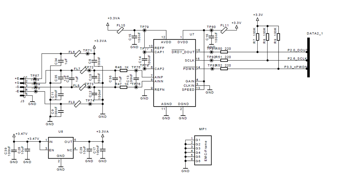
Could you please check if below connection of ADS1230 is correct? Thanks.

Best Regards.
Chen
This thread has been locked.
If you have a related question, please click the "Ask a related question" button in the top right corner. The newly created question will be automatically linked to this question.
Hi, expert,
Could you please check if below connection of ADS1230 is correct? Thanks.

Best Regards.
Chen
Hi Chen,
For the most part the schematic appears to be fine. It is not totally clear from observation why the ferrites are used in some cases. For example, +3.3VA appears to be coming directly from a linear LDO regulator and is only used for the AVDD, reference and excitation supply. Sometimes the ferrites will cause more issues than they are solving. Any inductance, even from ferrites, can cause issues by choking needed current during internal device switching and power up. This is true on the digital side as well. If additional filtering is required on the supplies, then it is recommended to create a low pass RC filter by replacing the FL10 and FL11 ferrites with low Ohm resistors (1-10 Ohms) instead.
Another consideration is the reference inputs. From a purely dc perspective the current path for both the excitation and the reference are similar. However from an ac perspective the excitation filtering is different from the reference input. To make the measurement truly ratiometric you would like to have the voltage for excitation to be the same voltage for the reference with respect to noise and drift. This may be challenging as there is filtering at the load cell connector. Ideally you would want the reference input filtering to be the same as the analog inputs.
C34 and C35 are 1uF caps and C9 and C11 are 100nF. It is not clear as to why these particular values are used, but C11 and C35 should be the same value as these capacitors are in the measurement path. The filtering intent is not clear, but I believe that the J3 pin 5 ground is meant as a cable shield connection. This ground would normally be at earth ground potential and may not be the same ground potential as your board ground. Generally you would want to isolate the noise from earth ground and board ground to prevent noise on the board ground. This can be accomplished by using a guard ring around the board that is at earth ground potential.
Best regards,
Bob B
Hi, Bob
Thank you very much for the schematic check. This application is used for electronic scale, and customer found the temperature drift is too large.
For example,
They will make AD1230 0mV as 0g,make 3.3mV as 30000g,
Then the temperature test is,
Under 20℃:
0mV 0g
3.3mV 30000g
So the SPAN is 30000;
Under -10℃:
0mV 0g
3.3mV 29980g
So the SPAN is 29980.
However the error is (29980-30000)/30000=-666.7ppm,
while the requirement of their product is less than 250ppm, but the error under -10℃ temperature shows -666.7-(-250)=-267%
Could you please help analysis if the temperature drift is normal? And what parameters cause the error? Thanks.
Best Regards.
Chen
Hi Chen,
Temperature drift affects the ADC primarily in 2 ways. One is with offset drift. The second is with gain drift.
The ADS1230 has typical offset drift of +/- 10nV/deg C drift. The offset drift can be removed by periodically issuing the self-offset calibration. I would suggest issuing the offset calibration prior to taking the -10 deg C measurement to observe the impact of making the calibration.
Gain drift has potentially a larger impact. The gain drift is +/- 4ppm/deg C. However this is drift is relative to full-scale range. Most load cells only use a small portion of the full-scale range so the impact of gain error and gain drift is not as large as it would be when the input is at full-scale.
The other factors are the drift of other system components and the load cell itself. Load cells come in a great variety of types and shapes and may or may not be temperature compensated.
In most precision scales that I am familiar with, the electronics are not operating at such temperature extremes so it is difficult for me to give an answer with what might be expected with respect to drift performance of the system.
If we back up a step, the noise of the ADC will also cause some issues. It is not clear what the expected scale resolution is, but it is not possible for the ADC to get better than 3g resolution at a gain of 128, data rate of 80sps and 3.3V analog supply/reference. To this point the affect of temperature is based on calculations with respect to some other calculations. It is not clear to me what calculations are being done to determine the outcome. To fully understand what may be going on I need to see the raw ADC codes without calculations to determine the drift performance of the ADC itself.
The datasheet graphs in Figures 9 and 10 help to show the offset and gain responses over the temperature range being used.
Best regards,
Bob B