A related question is a question created from another question. When the related question is created, it will be automatically linked to the original question.
If you have a related question, please click the "Ask a related question" button in the top right corner. The newly created question will be automatically linked to this question.
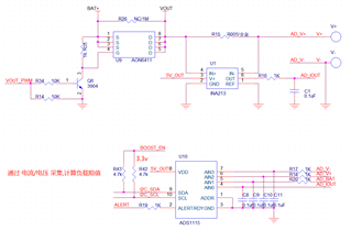
For the schematic, the ALERT/RDY pin is an open drain output and should have a pullup to 3.3V or VDD depending on the levels needed for the GPIO it will be connected to.
I'm not quite sure I understand your question about the output calculation formula. The ADC provides an output code directly proportional to the inputs. You can see an example of the LSB size (the voltage corresponding to a single code in the ADC) in Table 3 of the datasheet here: