This thread has been locked.

If you have a related question, please click the "Ask a related question" button in the top right corner. The newly created question will be automatically linked to this question.

DAC81408EVM: No output on every channel

Part Number: DAC81408EVM

I recently bought a DAC evaluation board, the DAC81408EVM, from TI.
My problem with this board is that I can't get an output voltage, no matter what channel I choose.

The communication with the DAC works fine, I attached a signal analyzer and confirmed that the communication to the DAC is ok and the communication backwards too.
The DEVICEID-register gives back the right value, 0x298.
After a reset command, all registers change their values to the ones that are stated in the data sheet. Except of the register
- 0x02, the bit 2 = 1, it is a reserved bit,
- 0x03, the bit 7 = 0, it is also a reserved bit.
These bits are flipped.

Writing to all registers works also fine, except of the registers
-0x0F
-0x14 to 0x1B
They don't update their value and there is no output voltage. I also tried the synchronous mode and send a LDAC command or the broadcast function, they wont update either.

The power supplies that are used have a voltage, measured at the board, of

V_io = 3.3 V
V_dd/V_aa = 4.92 V
V_cc = 10.06 V
V_ss = 0 V
GND = 0 V.

The jumpers on the evaluation board are set to

J9 1-2 (pin 1 is connected to pin 2)
J10 1-2
J11 1-2
J12 1-2


The minimalistic code only consists of:
...............................................................................................................

DAC(WRITE, 0x0E, 0b1010) // for the Power on Reset function
delay(50 ms)
DAC(WRITE, 0x03, 0x0A84) // set the device in active mode
DAC(WRITE, 0x09, 0xF00F) // turns on all DAC's

DAC(WRITE, 0x14, 0xF000) // writes 0xF000 to the DAC_0 Buffer
delay(50 ms)
DAC(READ, 0x14) // reads the value from DAC_0 ---> is 0 and not the 0xF000

...............................................................................................................

Cutting the power of the DAC an plug it in again does also not help.


I hope there is something that I have been missing.

  • Hi,

    Can you please post the scope shots of SPI frame? I think you forgot to attach the same.

    Can you measure the voltage at TP12? Do you intend to operate the DAC with internal reference or external reference? If its internal reference remove the jumper J11.

    Regards,

    AK

  • Hi,

    I wanted to use the DAC with the external reference which is included on the development board (REF5025AIDR), the measured voltage was 2.5 V.

    Your suggestion was to try the internal one (removed the jumper and turned the reference in its register). In this case the measured voltage was 0 V.

    The next five pictures are showing the communication which was described in my initial post with the DAC. My signal analyzer inverts the signal (confirmed with an oscilloscope). So the real signal is inverted in comparison to the uploaded pictures.  

    DAC(WRITE, 0x0E, 0b1010) // for the Power on Reset function
    delay(50 ms)
    DAC(WRITE, 0x03, 0x0A84) // set the device in active mode
    DAC(WRITE, 0x09, 0xF00F) // turns on all DAC's

    DAC(WRITE, 0x14, 0xF000) // writes 0xF000 to the DAC_0 Buffer
    delay(50 ms)
    DAC(READ, 0x14) // reads the value from DAC_0 ---> is 0 and not the 0xF000

    DAC(WRITE, 0x0E, 0b1010):

    DAC(WRITE, 0x03, 0x0A84):

    DAC(WRITE, 0x09, 0xF00F):

    DAC(WRITE, 0x14, 0xF000):

    DAC(WRITE, 0x14, 0xF000):

    DAC(READ, 0x14):

    The next one is showing the command to turn on the internal reference:

    DAC_TALK(WRITE,0x04,0x3F00):

    Regards,

    RR

  • Hi,

    How is your SPI read, is it working? Can you read back the register 0x04 and confirm 0x3F00 is written?

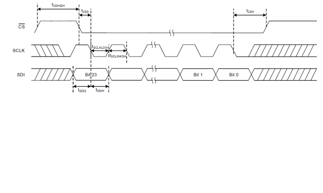
    Looking at the SPI frames, I have a feeling that the SPI mode you are operating is not mode 2. Our device supports SPI mode 2 of operation. Please change according to datasheet.

    Basically when /CS goes low, SCLK has to be high state and it has to obey the timing requirement tcss. Data will be clocked in on the falling edge of SCLK. I cannot verify this in your SPI frames with inverted logic. Can you please post scope shots?

    Regards,

    AK

  • Hi,

    The SPI read is working, at least at some registers. On this one (0x04) the read after the write is 0, should be 0x3F00.

    I changed the the SPI mode to SPI mode 2.

    The following picture contains a read, write, read operation.

    Serial.println(DAC_TALK(READ,0x04,0),HEX);
    delayMicroseconds(5);
    DAC_TALK(WRITE,0x04,0x3F00);
    delayMicroseconds(5);
    Serial.println(DAC_TALK(READ,0x04,0),HEX);

    Regards,

    RR

  • Hi RR,

    This plot is not readable. Can you please post one SPI frame with proper timings on the scope. No need to post multiple frames. Just a single write frame to address 0x04 with data 0x3F00

    Regards,

    AK

  • DAC(WRITE,0x04,0x3F00):

  • Hi,

    In this why SDI is going high in the second 8 bit frame start? Please note that data is latched on the falling edge of SCLK

    Regards,

    AK

  • The SDI goes high because the microcontroller only sends 8 bit at a time. So the 24 bit word has to be split up into 3 parts.

    During each transmission the MOSI goes high by default. 

  • Hi,

    First we need to make sure that the read is working for all registers. This way we can be sure that the write has happened. Can you configure your MCU to send 3 bytes of SPI frame without any gap? Although this shouldn't matter, I just want to do it as a debug.

    Also after enabling internal reference, you didnt get 2.5V right? This points to SPI communication issue. Can you please make sure SPI is working correctly from your MCU side?

    Make sure /LDAC, /CLR, /RESET pins are pulled high to VIO in the EVM. Jumpers J2 and J3 are open

    Regards,

    AK

  • Hi Akhilesh,

    Thank you for your help, the DAC is now working.

    I am not sure what the problem was, or what has changed. 

    Still it is working, thanks again for your support.

    Regards,

    RR