This thread has been locked.

If you have a related question, please click the "Ask a related question" button in the top right corner. The newly created question will be automatically linked to this question.

ADS8556: Unintentional busy without CONVTST

Part Number: ADS8556

Dear Sir,

I have used ADS8556 and faced with some unintentional busy signal without CONVST high, plz refer to below attached fig

fist yellow busy and second blue is CONVST, as you can see, after CONVST goes to low, unexpected busy occurred and its level is too small to lead to power down mode I guess,

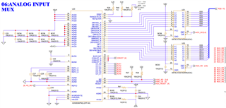
And our schematic design is as follows,

During operation, after some making switching mechanical contact it goes to power down mode as follows,

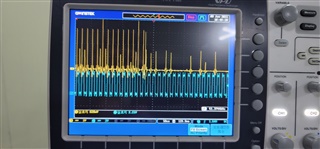
As you can see above fig., around a middle of, busy signal goes to unintentional high after CONVST low and it makes partial power down mode and  ADC8556 is not working before RESET signal

Could you recommend if you have a experience to solve like this?

Is there any risk on our schematic design above?

Your prompt reply will be highly appreciated.

  • Hi Kayhen,

    In your first timing graph, the higher pulses on the yellow signal are correct BUSY output because they are going to high (conversion) when the CONVST signals are issued (even I can not check the width of the pulse because your timing does not show it). However, the lower pulses on the yellow signal are incorrect, so something was wrong so that the ADC output these additional incorrect BUSY pulses.

    I checked your schematic, there are two issues:

    1. You are splitting the ground for AGND and BGND, do you have any connection for them? I can not see it in your schematic.
    2. What's your maximum and minimum analog input signal on CH_A/B/C_x pins? You HVDD should be at least 1.5V higher than your maximum input signal and your HVSS should be 1.5V lower than your minimum input signal. Right now you are using +/-5V for HVDD and HVSS which probably did not meet the requirements.

    Best regards,

    Dale